I decided to take this charger apart when I noticed some weird stuff happening with my phone when connected to the charger (touchscreen not working properly - probably high EMI from the charger).
This is just a generic USB charger that plugs into an European socket and has an USB output on the side.

The charger (click for full resolution)

Inside (click for full resolution)

Circuit board, top side (click for full resolution)

Circuit board, bottom side (click for full resolution)
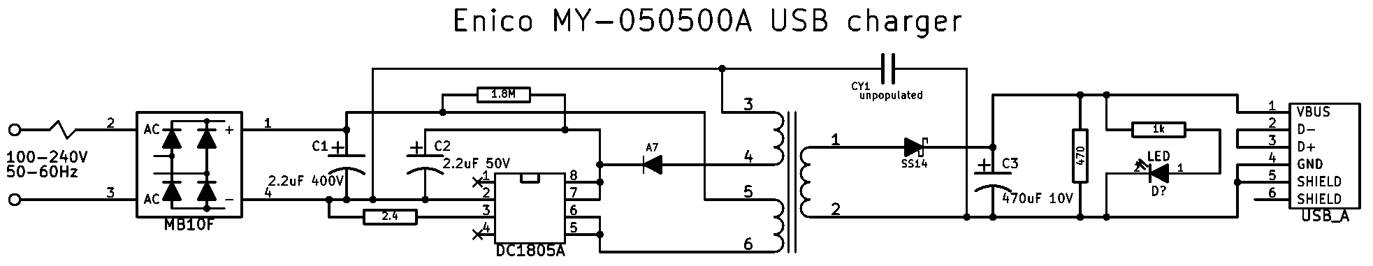
Schematic (click for full resolution)
Unlike many cheap chargers, this charger is not based on a self oscillating circuit. A special chip is used here, marked "DOCN DC1805A CG7P1C 1HJ". I haven't managed to find a datasheet. This IC is in an 8-pin surface mount package.
The distance between primary and secondary sides is in the ballpark of 2.5mm, which seems a bit too low for European safety standards.
The Y capacitor between the primary and secondary side (marked CY1) is also missing. The charger makes huge amounts of electromagnetic interference, interfering with my amplifier when any longer cable is connected to the USB output. It also interferes with the (capacitive) touchscreen on my phone. This capacitor is supposed to short the high frequency noise caused by spikes from the primary being capacitively coupled to the secondary coil, which causes problems with many devices. These capacitors are usually in the low 100s of pF range. I added a proper capacitor in place and it solved the problem. It must be a proper Y-rated capacitor for safety reasons!
The output capacitor (C3) is marked "Low ESR" and the ripple waveform seems fairly strange, it's mostly quite low and looking similar to a sawtooth-like wave with some distance between impulses (this is most likely a discontinuous mode flyback power supply), but there are big spikes/ringing on the positive-going edge of the "sawtooth". The distance between the positive pin of C3 and the rest of the circuit is fairly high.
Notice the "fuse" on one of the mains inputs, which is just a thin trace that is apparently designed to blow when too much current passes through.
There is also no proper filtering or inrush current limiting on the mains input
This is a product that apparently violates several standards and causes a lot of interference. It's hard to say how good/bad the insulation of the transformer itself is. To me it definitely doesn't seem like a well designed product. However, it's still better than many other Chinese chargers.