This is a device designed for testing saturation current of various inductor and measurement of parameters of inductor cores using current up to 50 A.

Power board schematic (click for full resolution)
The power board consists of a capacitor bank (6x 4700 µF) capable of delivering short high current pulsed, MOSFET drive circuitry (R2-R5, Q1, Q2, C9), power MOSFETs (Q4, Q5), a sense resistor (R6), diode (D2), overcurrent detection (Q3 and parts around Q3). The driver board is connected to J2, the measured inductor is connected to J2, J3. The power is connected to J1 - 12 to 15 volts from a current limited (e.g. bench top) power supply.
Working principle: the driver board switches pin 2 of J2 on (Vcc, logical 1). MOSFETs Q4, Q5 turn on. Transistors Q1, Q2 are wired as voltage followers and are used to strenghten the gate drive to ensure fast turn-on and turn-off. As Q4, Q5 switch on, current throught the device under test starts to rise (rate of change of current is dependent on inductance - less inductance, faster rise of current). As the current rises, the voltage across R6 (current sense resistor) starts to rise. This voltage is displayed on an external oscilloscope (connected to J5, 10 mV/A) and sensed by the overcurrent protection circuit (if the voltage reaches over approximately 600 mV - corresponding to 60 A - Q3 turns on and the driver electronics board switches the output back to log. 0, turning Q4, Q5 off). Higher inductance will correspond to slower rise of current. When saturation is reached, the current starts rising faster, which is visible on the scope. The sense resistor must be relatively robust (although the average current is low, the peak current is fairly high), but it also must have low parasitic inductance. When the MOSFETs switch off, the resulting spike "returned" from the inductor must be clamped - this is done using diode D2 (which must be also able to handle high peak current, here it's also placed on a tiny heatsink), which clamps the voltage to around 1 volt - the current slowly falls as the energy stored in the inductor turns into heat in the diode. MOSFETs Q4, Q5 should have low on-state resistance. All power traces should be as short as possible.
The inductance can be approximated with the formula L=V*Δt/ΔI, where V is the voltage on the device under test (approximately the power input voltage, with higher currents, the voltage drop across the resistances of the device itself starts to play a role). Δt and ΔI are the difference in time and current - when a point on the oscilloscope around which we want to calculate the inductance is set, Δt and ΔI correspond to the difference of current (calculated from the voltage - 1 A/10 mV) between two nearby points - cursors can be used on a digital oscilloscope.
The saturation current can be also read out from the measured waveform - when the current starts to rise more rapidly after some current was reached, the inductor is going into saturation.
Wires going to the measured inductor must be as short as possible, each millimeter adds approximately 2 nH of inductance.

Driver board schematics (click for full resolution)
This board consists of an oscillator, flip-flop, under-voltage lockout circuitry and other parts. It's connected to the power board through J3.
The oscillator is based on the NE555 integrated circuit and operates with very low duty cycle (to prevent overheating of the device). Resistors R3, R4 set the off time. A potentiometer (10 kΩ) connected to J1 sets the on time. A higher on/off time range can be set using a switch connected to J2.
The flip-flop U2a (U2 = CD4013, dual CMOS flip flop) switches its output to log. 1 on the rising edge of the oscillator output pulse. Its RESET input however has higher priority (the output can't be set to log. 1 using the C, D inputs when this input is activated) and is able to be activated by several ways. Q3, D8 together with other parts reset the flip-flop on the falling edge of the oscillator output pulse. It can also be reset by the overcurrent circuit (based around Q1) or the under-voltage circuit (based around Q2). A switch is present in series with the Zener diode (D4) in order to be able to deactivate the device (stop generating pulses). The output of U2a goes to the MOSFET driver. The inverted output of U2a is connected to J5 (synchronization output for oscilloscope trigerring, ideally on falling edge) through some parts to shape the pulse. I used a small isolating transformer (~10:10 turns on a small ferrite core) between J5 and the oscilloscope due to some problems with different potential on the grounds of the two boards (due to wiring resistance) causing output offsets. The other half of U2 (U2b) is used for overcurrent signalization - it keeps the overcurrent LED on until the next oscillator cycle.
Capacitors C4, C6 should be placed close to the power pins of U1, U2.
Both boards are built on single-sided PCBs containing both THT and SMD parts. I accidentally haven't left enough place near the traces on one of the boards and had to use plastic insulating washers. BNC connectors are used on the output. KiCad files are available here.
Modifications - March 2021: the power switch was added to the schematic diagram (SW1). Diode D10 was added and values of some parts near Q3 were changed. Modified files for KiCad are here, old files are here. The quality of the circuit diagrams in this article was improved. A photo of the bottom side of the driver board was added, however it might slightly differ from the files available for download here - the board was modified after it was made and the modifications were added to the design files retrospectively. Some shielding was added to the front panel - grounded copper tape under the potentiometer and switches. Sadly the front panel plastic got slightly warped during the modifications.
Using the measured quantities, the following can be calculated:
- inductance L [H] = V*Δt/ΔI [V, s, A],
after winding a few turns on an unknown core:
- maximum magnetic flux density Bmax [T] = V*I*Δt/(N*S*ΔI) [V, A, s, -, m2, A], calculated from quantities measured right before saturation. S is the core cross-section area, N is the turn count.
- permeability μabs = L*l/(N2*S) [H, m, -, m2], where l is the effective core length. Relative permeability μr can be calculated by dividing the absolute permeability by 4*π*10-7
These equations are based on the following equations: uL(t) = diL(t)/dt, H=N*I/l, B=μ*H.
Inductance per turn can be determined by dividing the inductance by the number of turns squared. Saturation current for one turn can be determined by multiplying the number of turns by the saturation current - then calculated for another winding on the same core by dividing the saturation current for one turn by the number of turns.

Entire device (click for full resolution)

Insides (click for full resolution)
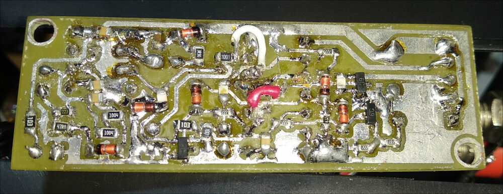
Bottom side of driver board (click for full resolution)

Measurement (Isat≈15 A, L≈60 µH, 10 A/div, 8 μs/div) (click for full resolution)
Warning - as always, this information is provided with no warranty. If you decide to build this device, you do so at your own risk.