Risk of injury. You do everything at your own risk - I don't take any responsibility for any property damage, injuries or other harm caused by applying any of the information here.
This is a digitally controlled high voltage power supply. The output voltage range is 500 V-5 kV. It includes an isolation test function (current measurement, resistance calculation).

Schematic diagram (click for full resolution)
The device is powered from a 12 V, ≥2 A power supply through the connector J6. The power input is fused (F1) and protected against reverse polarity (D3) and filtered with C7. The basic input circuitry is followed by an LCR filter (L1, R19, C11) and voltage regulator (U3 - 7805 and capacitors C14, C18, C22).
The control logic part is based on the ATmega328p microcontroller (U1), which is clocked by the crystal Y1 (16 MHz). Its AVCC input is filtered using FB1, C9. Button inputs are filtered and debounced using RC networks (R20-22, C10, C12, C13). Voltage feedback is connected to J9 through an external 120 MΩ resistor (divided into several sections, the last 40 MΩ section is shielded), the internal ADC is used to sense the voltage. The lower part of the divider consists of resistor R25 and C20. Current measurement for isolation measurement (input J1) is implemented using a selectable shunt (resistors R1-R3). This input is protected by the varistor MOV1 and a fast clamp circuit (R4, R6, Q1 - B-E junction in "Zener-like" mode). Output current sensing is implemented by transistors Q7, Q8 and parts around them. The circuit gets activated at several mA (safety feature), the current can be lowered to 2-3 mA by changing R26 and C21 to around 10 kΩ and 100-330 pF. The ~OCD node is also connected to a circuit that senses the primary/MOSFET current. Parts C21 and R26 reduce noise on this node (the pull-up in U1 isn't enough by itself).
The power part is driven by a PWM signal at around 31 kHz. It consists of a level shifter (Q2, Q3 and nearby parts, 5 V to 12 V), follower/current boosting circuit (Q4, Q5) to drive the gate of the switching transistor (MOSFET Q6), the power MOSFET itself, which drives the primary of a small high voltage transformer (J3, J4) and an over-current detection circuit. The switching speed of Q2 is enhanced using capacitor C1 (providing a current pulse when changing state). Turn-off of Q3 is made faster using a Schottky diode (D1), which prevents saturation. The collector of Q3 goes to the bases of Q4, Q5, which work as followers (current amplifiers) and drive the main MOSFET gate through R9. The MOSFET current is sensed using R10 (0.22 Ω) between its source and ground, if a certain voltage drop is present, then the comparator U2A connects the ~OCD node to ground, this goes to the MCU and activates an interrupt routine handling over-current protection. Noise/fast spikes are removed using R12, C2. Maximum current can be set between approx. 1.5 to 4 A (the trimpot RV1 sets the voltage level necessary to activate the comparator). The second comparator in U2 is used for +12V rail undervoltage detection. The MOSFET is heatsinked (the heatsink is placed directly on board, connected to J2 and isolated from the FET with a sil-pad). The MOSFET is avalanche rated and there is no external circuit to absorb spikes from the transformer.
A small HV transformer from a photocopy machine is used here. It is connected to the circuit board using a short shielded cable (the shield is connected to J3, internal conductor to J4). It operates in flyback mode (careful with phasing, the high voltage output pulse polarity is reversed relative to "charging" - Q6 on). The primary is connected to J3, J4. The transformer has a built-in diode. Its positive output goes to a 5 nF, 5 kV capacitor. The negative, cold end is connected to HVRTN and the 5 nF capacitor. A high voltage resistor (5.6 kΩ) is connected between the HV capacitor and load to prevent a huge current spike due to discharge of the 5 kV capacitor. The negative pole of the load is connected to GND as close as possible to J5, D2, C5. In insulation resistance measurement mode, the load is connected between HV +OUT and J1 (MEASURE). An external protection network must be placed between J1, J11 and the tested load. Both GND and the current measurement input are broken out on the back panel using banana jacks. The GND jack is connected directly to the case shielding using copper tape. For protection, a 200 volt gas discharge tube is connected between the current measurement jack and the ground jack. The current measurement input then goes through a differential-mode filter (several turns on ferrite) to limit di/dt, and also through a common mode filter (both the current input and GND from the banana jacks - wound using a twisted pair on a ferrite core) to connectors J1, J11 on the circuit board. The circuit board ground node is also connected to the shielding.
Shielding is done using copper tape, which is applied to the panels, and under/over/near the circuit board. Everything is placed inside an ABS enclosure.
A character LCD (16x2, HD44780 - lines VCC (display VDD), GND (display VSS), contrast, E, RS, D4-D7, others are tied to ground) and buttons (BTN1-3, switching to ground) are connected to the connector J8.
The microcontroller is programmed through J7. The program is written in Arduino IDE. Speed-critical parts use direct port/register manipulation. Regulation is done using a PID loop. The PID loop runs at approx. 8 kHz, which isn't too much of a problem here due to the fairly large output capacitance. The PID coefficients should be tuned for minimal overshoot and maximum speed, accuracy and stability. Fuse settings for the microcontroller are mentioned in the source code.
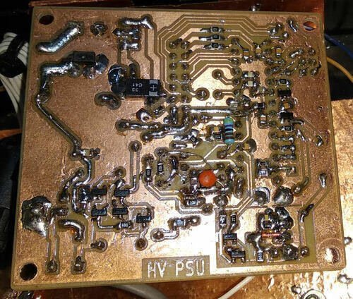
A single sided-board is used (with wire jumpers). It was made by photo transfer and persulfate etching. Both SMD and THT parts are used. Some care is needed regarding layout (EMI susceptibility). Capacitors C2-C4, C6, C8, C9, C11, C14, C15, C21-C24 must be placed as close as possible to corresponding circuits. Some modifications have been done to the board after it was made, these modifications are included in the KiCad project files.
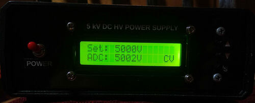
The voltage is adjusted using the UP (BTN1) and DOWN (BTN2) buttons in 50 V steps. Voltages under 500 V can be set, but are not very accurate. The SEL (BTN3) button switches between voltage adjustment mode and resistance/current measurement (approximate, 50 nA to 1 mA, >500 kΩ). To enter calibration mode, hold SEL during startup and then rapidly press it after being prompted to do so. UP/DOWN adjust the displayed quantity, SEL moves to the next one. The calibration data is saved into the internal EEPROM.
Warning: the construction displayed below isn't optimal from a safety point of view. If you decide to build this (or similar) device, you do so at your own risk.
Arduino code (December 2020)
KiCad files (December 2020)
ZIP archive - KiCad, program - old version (February 2020)

Inside (click for full resolution)

Running - voltage display (click for full resolution)

Running - resistance and current display (click for full resolution)

Back panel (click for full resolution)

Circuit board underside with added components (click for full resolution)