
The entire device (click for full resolution)
This is a device designed to measure the capacity (mAh, Ah) of rechargeable batteries. It can also be used as an adjustable current dummy load - this can be useful for power supply testing, etc.
There are two circuit boards (logic board, load board). The logic board is based on the ATmega328P microcontroller. There also are some connectors (for the power input, display, dual-color indicator LED (not implemented in the firmware so far), button inputs, buzzer, programming (ISP)). There are also two voltage regulators - a 9V regulator for the load board and a 5V regulator for the microcontroller. On the load board, there's and op-amp, a power MOSFET and again some connectors (one to connect to the logic board, 4 fastons (2x +, 2x -) to connect the device under test, and a terminal block connector for a cooling fan).
A regular 20x4 character LCD display (J204A) is used here.
I took the idea (and part of the circuitry - especially the power/load part is almost the same as in his battery analyzer) from Danyk's battery analyzer (link here), the parameters are almost the same, however my version has completely different code, many other differences + some more features.
The function principle is very simple - in capacity measurement mode, the battery is discharged with a constant current until the pre-set cutoff voltage is reached - the calculation is very simple: C=T*I [Ah, h, A]. In internal resistance measurement mode, the device does 2 voltage measurements at different currents. The calculation is also very simple: Ri=ΔV/ΔI.
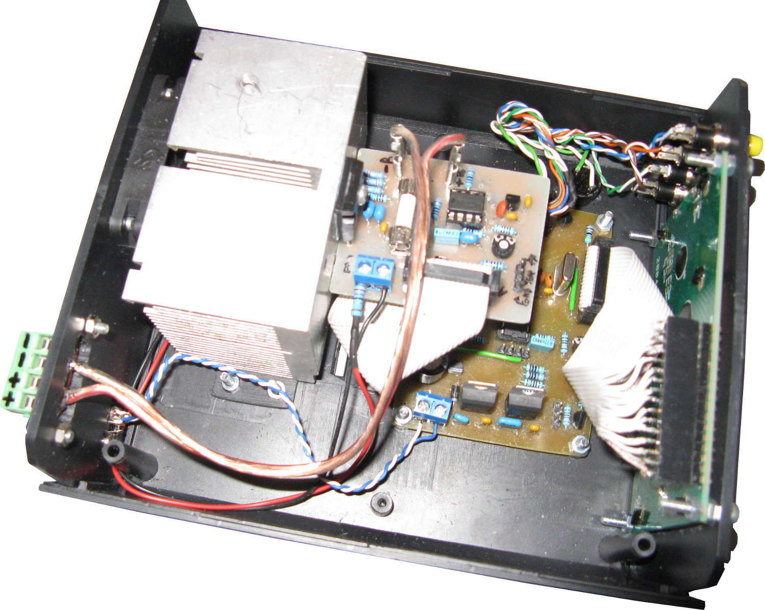
Inside (click for full resolution)
The logic board and the heatsink (which is epoxied to a small "carrier" plastic board) are mounted inside the box using M3 screws and nuts. There are some standoffs under the logic board.
Everything is mounted in a project box (KP 9 V type, dimensions: 150x179x70 mm)

Front panel (click for full resolution)
The display and buttons are mounted on the front panel.

Back panel (click for full resolution)
You can see a fan protection grill (the fan is a regular 50 mm fan, SUNON EE50101S1-999) and the battery & power supply connectors on the back.
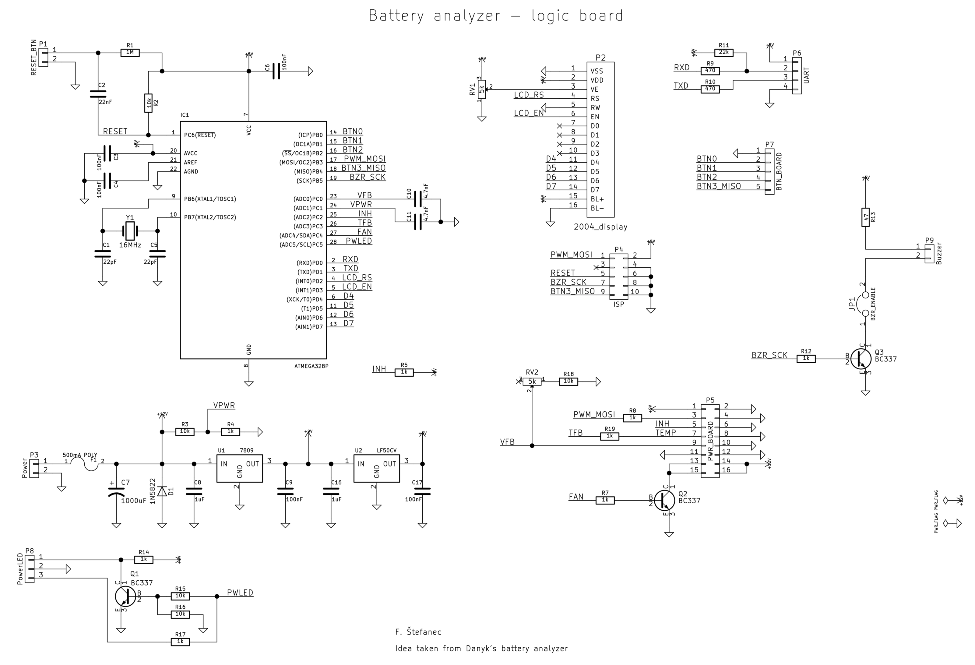
Logic board schematic diagram (click for full resolution)
This board carries the ATmega328P microcontroller, many connectors (for power, programming, load board connection;, display, UART (not implemented in the FW yet), buttons, buzzer), the power regulators and other necessary circuitry around the microcontroller.
The power circuitry consists of the connector C3, the fuse F1 (a resettable PolyFuse), the voltage regulators (U1, U2) and related capacitors - C8, C9, C16, C17. The 5 volt regulator (U2) should be as precise as possible.
The microcontroller uses a crystal as the clock source (Y1 in the circuit diagram). There are also some more capacitors - C3-C6, C10, C11 - for decoupling and filtering purposes.
The built-in ADC has only 10b resolution - I use oversampling to gain an extra bit.
The microcontroller's UART interface is connected to the pin-header P6, but it's not yet implemented in the firmware.
The connector P2 is used for display connection. The pin numbering matches the pinout of regular 16-pin HD44780 compatible display modules.
For programming, the connector P4 is used. Any standard ISP programmer, such as USBasp, can be used.
The buttons are connected to P7, the pinout is: 1:GND 2:OK 3:Down 4:Up 5:ESC. The buttons switch the pins 2-5 to ground.
A small magnetoelectric buzzer is used here (for feedback/signalization). It's connected to P9.
There also are two trimpots: RV2 for voltage measurement voltage divider adjustment, RV1 for display contrast adjustment.
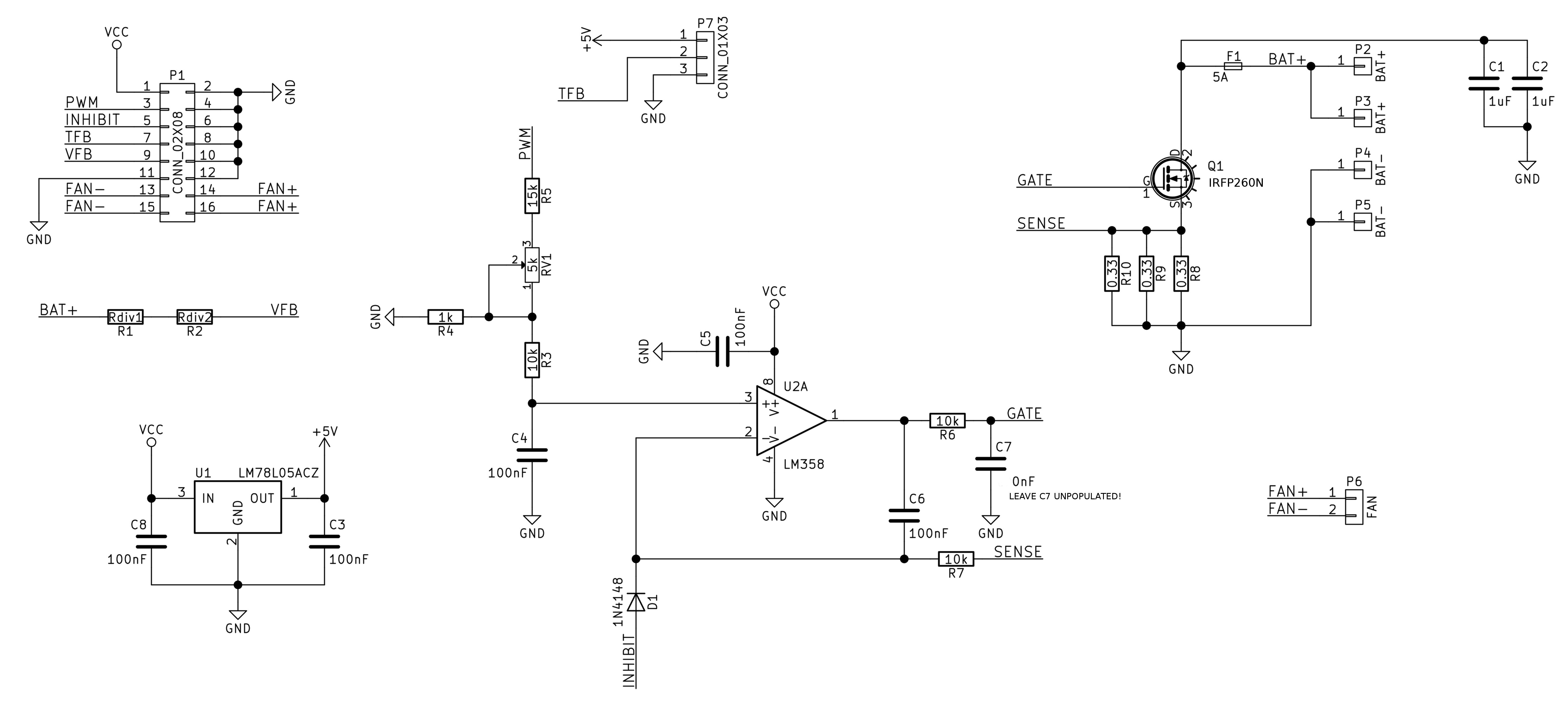
Load board schematic diagram (click for full resolution)
This circuit board is connected to the logic board using a short flat cable.
A power MOSFET (IRFP250, used in linear mode) is used as the load.
This board takes power from the 9 volt regulator - 5 V might not be enough for the power MOSFET (IRFP250N). The maximum power dissipation of the power MOSFET is 51 W (20 V, 2.55 A). A CPU heatsink is used for cooling, together with a cooling fan, connected to the connector P6.
Current regulation is done by the op-amp U2 (LM358). There's a circuit (consisting of C4, R3, R4, R5, RV1) to convert the signal (PWM) from the microcontroller. The current can be adjusted using RV1. The time constant of the RC circuit consisting of C4, R3 should be at least 30x times higher than the period of the PWM signal - therefore, C4 should have a value of at least 100 nF, I have a 1 µF capacitor in place, but any higher value will result in a big increase of the response time.
Current sensing is done using R8, R9, R10. The voltage on those resistors will be around 0.28 V at full current. This is connected to the inverting input of the op-amp.
The op-amp used here (LM358) has fairly bad parameters (high offset), therefore the regulation is very inaccurate at low currents. It would be much better to use a better op-amp.
A temperature sensor can be connected to P7, but it's not yet implemented in firmware.
100 kΩ resistors can be used in place of R1 and R2. They form a part of the voltage feedback divider together with more resistors on the logic board.
The updated firmware can be downloaded at the end of this page.
I added firmware support for temperature monitoring (a LM35 sensor can be connected to the header on the discharge board: +5V to Vcc, GND to GND and TFB to the sensor output. A resistor (approx. 2-10 kΩ must be connected between the sensor output and GND). There are two different HEX files (for use with/without the sensor in place) and for an indication RG LED.
If the sensor is installed and the correct firmware is flashed, the fan becomes temperature controlled. >55°C = fan turns on, <48°C = fan turns off, ≥78°C = emergency halt. These values can be changed in the config.h file (the project must be recompiled after that).
mWh and power measurements/calculations are added (use UP/DOWN to switch between mWh+power/mAh+current display).
The accuracy has been improved (especially the accuracy of internal resistance measurement) by using more samples during averaging/oversampling. A critical display error that used to occur when measuring high capacities/high times has been fixed.
I did some hardware modification as well - added the temp. sensor & LED, added banana plugs and a screw terminal block on the front panel.

Entire device (click for full resolution)

LM35 sensor mounted close to the power FET (click for full resolution)
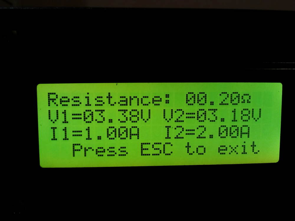
Example of internal resistance measurement (click for full resolution)

Example of mWh display (click for full resolution)