This is a module designed to demonstrate the necessity of using decoupling capacitors with most integrated circuits. It is possible to connect or disconnect decoupling capacitors on this board using jumpers. Disconnecting them leads to big voltage drops on the power rail of the integrated circuit used here. These capacitors, typically in the range of some nF to some µF, work as a local power supply capable of covering short current spikes - preventing voltage drops and spikes. If current going through an inductance (e.g. a PCB trace) changes quickly, it leads to a momentary voltage drop or spike. Decoupling capacitors can compensate this and should be placed as close as possible to the respective circuit, optimally "into the way" of the power traces. Not using decoupling capacitors can lead to stability or EMI issues even in case the circuit seems to work. In the worst case, the circuit can get damaged by resulting voltage spikes.
A NE555 timer operating in astable mode is used as the tested integrated circuit. Even though this is a very old IC, it tends to draw short (several tens of ns) pulses with a magnitude of several hundred mA when switching the output state. A long trace (40 cm) is present on the board, which simulates the inductance of a cable - it simulates a situation where the circuit is powered from a power supply through too long wires. Connecting or disconnecting the onboard capacitors can be used to demonstrate their effect on the power integrity on the power pins of the IC.
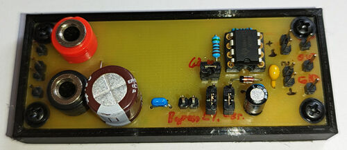
Finished module (click for full resolution)
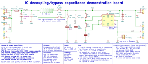
Circuit diagram (click for full resolution)
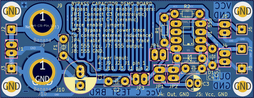
PCB layout (click for full resolution)
Pin headers and banana connector sockets are present as power input connectors. The input is protected using F1. Capacitors C1, C2 ensure a low power supply impedance regarding moderate to high frequency AC signals. The input voltage then goes into the oscillator itself through a long trace that can be enabled using the jumper JP4 or disabled using JP3. The 40 cm long trace has an inductance of a few hundred nH. When neither JP3 or JP4 is connected, an external inductor can be connected in the place of JP3. The NE555 IC is protected using a Zener diode against voltage spikes.
Jumpers JP1 and JP2 are used to connect or disconnect the capacitors: JP1 controls the capacitor C4 (100 nF ceramic), JP2 controls JP3 (10 µF electrolytic). IC Vcc/GND waveforms can be measured on pin headers J6+J8 (or J5), the oscillator output can be measured on J7+J8 (or J6).
The oscillator frequency is controlled using R1, R2, C5.
The voltage drop on the power trace is (as long as the signals aren't changing fast enough so that the trace has to be considered a transmission line, and its capacitance can be neglected) determined by its resistance, inductance, and the current flowing through the trace. The resistance plays a larger role for DC currents, while the inductance plays a larger role for pulsed current. The voltage drop on an inductance is given by the rate of change of current (${\mathrm{d} i(t)}/{\mathrm{d}t}$), the voltage drop on a resistance is given by the resistance and the current.
${v}_{R}(t) = R \cdot i(t)$
${v_{L}(t)} = L \cdot \dfrac{\mathrm{d} i(t)}{\mathrm{d} t} \rightarrow \Delta v_{L-pulse-max} = L \cdot \mathrm{max}({\dfrac{\mathrm{d}i(t)}{\mathrm{d}t}})$
Considering a trace with an inductance and resistance of 200 nH and 0.5 Ω, a DC current of 100 mA or a pulsed current with a rate of change of 100 mA/10 ns would create the following maximum voltage drops:
${\Delta V}_{R-DC} = R \cdot I = \textrm{0.05 V}$
${\Delta v_{L-pulse-max}} = L \cdot \mathrm{max}{({\dfrac{{\mathrm{d}}i(t)}{{\mathrm{d}}t}})} = \textrm{2 V}$
Some integrated circuits (switching mode converters and complex logic like processors and FPGAs) can draw currents with a rate of change in the order of A/ns - a fraction of a nanohenry plays a significant role in such a case. The inductance of a 1 mm wide trace placed 1.5 mm (a fairly common PCB thickness) above a wide conductive plane through which the current returns is about 0.5 nH per mm.
An electrolytic and a ceramic capacitor are used on this board. The electrolytic capacitor has a much higher equivalent series resistance even though it has a much higher capacitance → a higher voltage drop can be seen. A small damped oscillation can be seen when only the ceramic capacitor is used (due to its low ESR, it resonates with the trace inductance).
In practice, electrolytic capacitors aren't typically used in this position (covering very short current draw pulses) on their own, but are used as "bulk" filtering for longer pulsed current draws, and/or to dampen oscillations. Capacitors also have a certain self-resonant frequency (SRF) given by their parasitics (inductance), at which their impedance is lower, and a combination of several different (e.g. 1 nF and 100 nF) ceramic capacitors is sometimes used to cover a wider frequency range (the higher the rate of change in some signal → the higher the frequencies contained with a significant amplitude in the signal). The critical frequency, according to which the capacitor with the lowest capacitance can be selected, can be estimated roughly as $f = {\textrm{0.35}/t_{edge}}$. Some ICs have many power pin pairs, where each pair requires one or more decoupling capacitors.
This board is designed as a single copper layer board with THT parts for easy manufacturing at home or in education contexts. Some SMD parts are added on the bottom to improve some parameters (see schematics).
Regarding the 555 IC and its variants, more modern CMOS variants tend to draw lower peak currents.
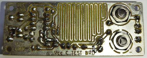
Bottom side of the PCB (click for full resolution)
Voltage drop measurement:
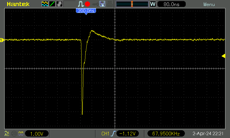
TI NE555, no capacitor, 80 ns/div, 1 V/div (click for full resolution)
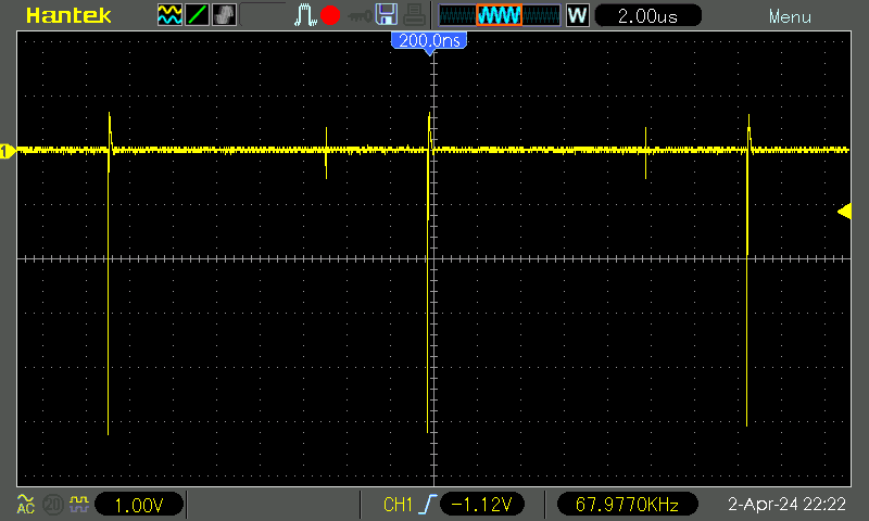
TI NE555, no capacitor, 2 µs/div, 1 V/div (click for full resolution)
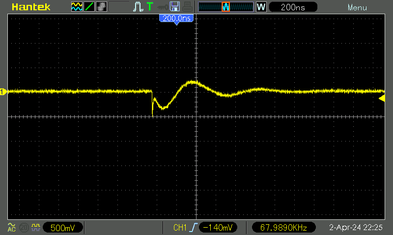
TI NE555, ceramic capacitor, 200 ns/div, 500 mV/div (click for full resolution)
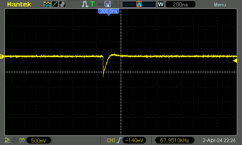
TI NE555, electrolytic capacitor, 200 ns/div, 500 mV/div (click for full resolution)
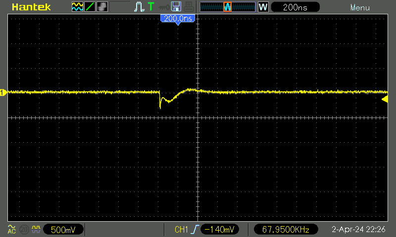
TI NE555, combination of capacitors, 200 ns/div, 500 mV/div (click for full resolution)
Details - 100 mV/div:
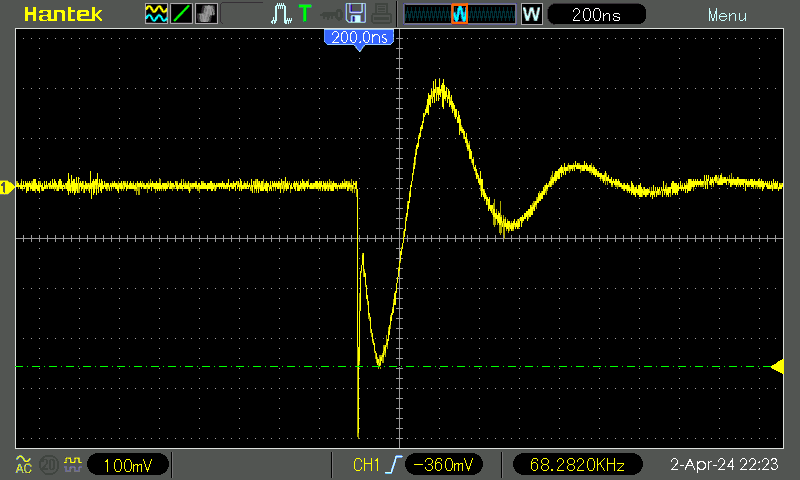
TI NE555, ceramic capacitor, 200 ns/div, 100 mV/div (click for full resolution)
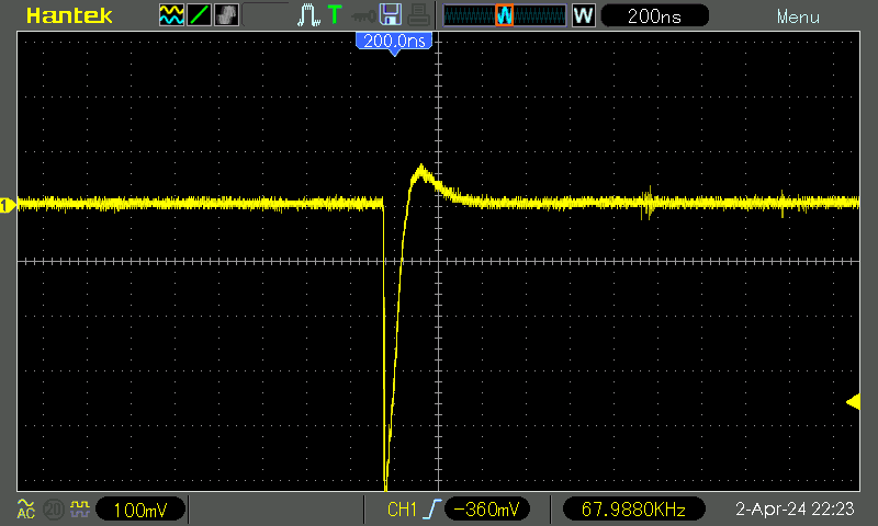
TI NE555, electrolytic capacitor, 200 ns/div, 100 mV/div (click for full resolution)
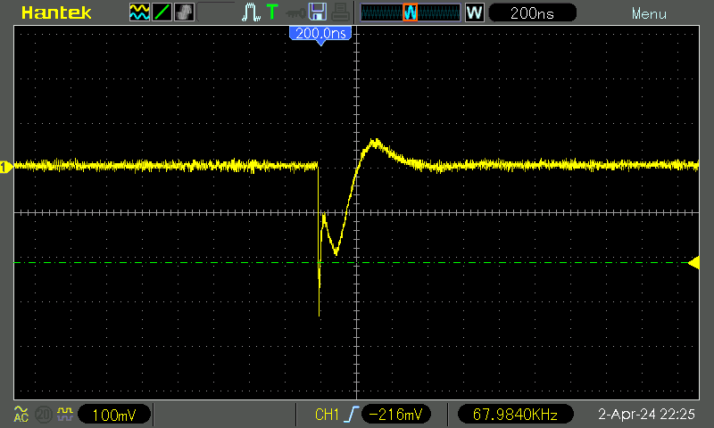
TI NE555, combination of capacitors, 200 ns/div, 100 mV/div (click for full resolution)
Voltage drop measurement:
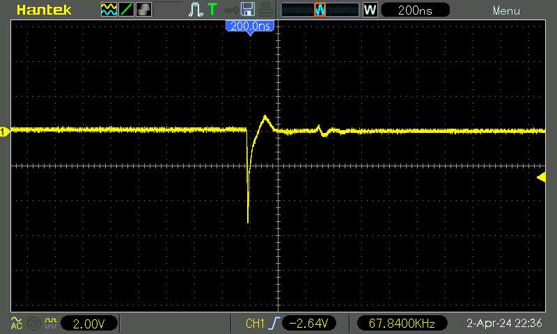
TI NE555, loaded, no capacitor, 200 ns/div, 2 V/div (click for full resolution)
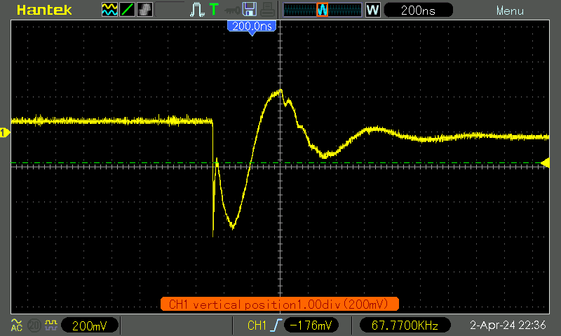
TI NE555, loaded, ceramic capacitor, 200 ns/div, 200 mV/div (click for full resolution)
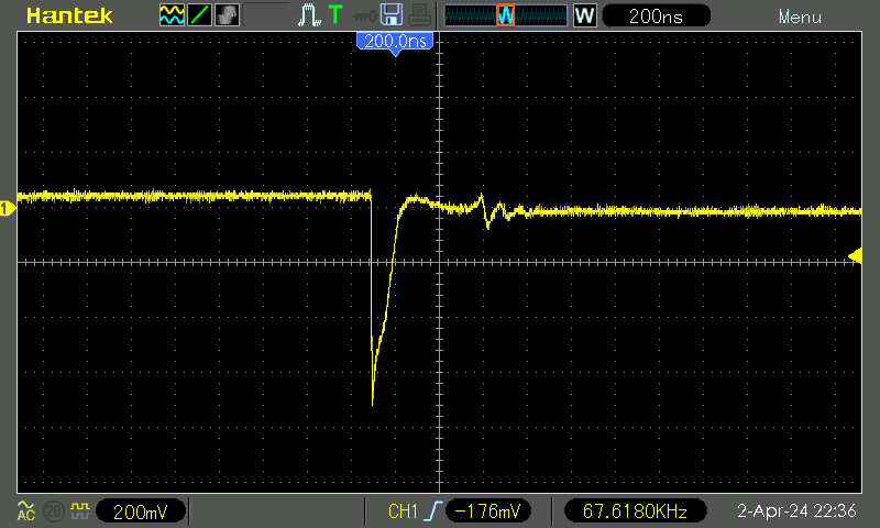
TI NE555, loaded, electrolytic capacitor, 200 ns/div, 200 mV/div (click for full resolution)
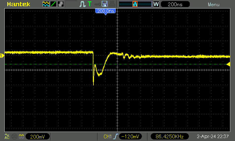
TI NE555, loaded, combination of capacitors, 200 ns/div, 200 mV/div (click for full resolution)
NE555 bought on Aliexpress, unknown manufacturer, logo similar to TI (fake/clone):
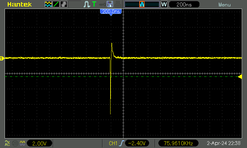
Unknown NE555, no capacitor, 200 ns/div, 2 V/div (click for full resolution)
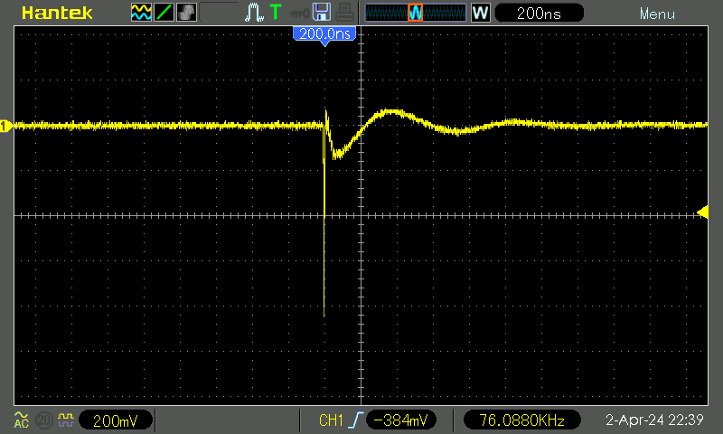
Unknown NE555, ceramic capacitor, 200 ns/div, 200 mV/div (click for full resolution)
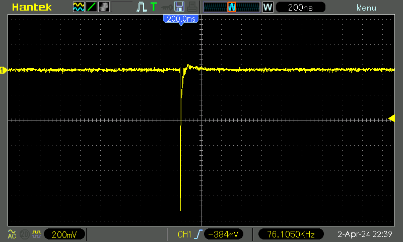
Unknown NE555, electrolytic capacitor, 200 ns/div, 200 mV/div (click for full resolution)
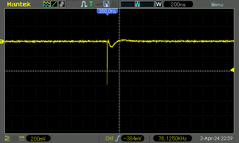
Unknown NE555, combination of capacitors, 200 ns/div, 200 mV/div (click for full resolution)
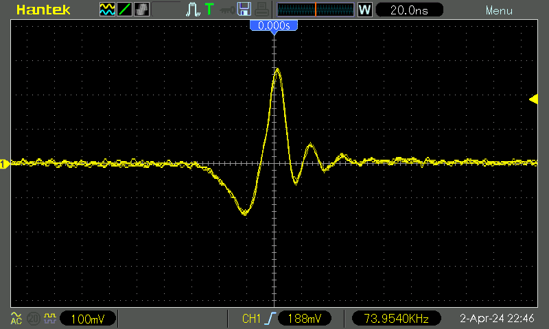
ICM7555, no capacitor, 20 ns/div, 100 mV/div (click for full resolution)
Archive - KiCad project, Gerber files, STL for 3D printing of the bottom casing.