
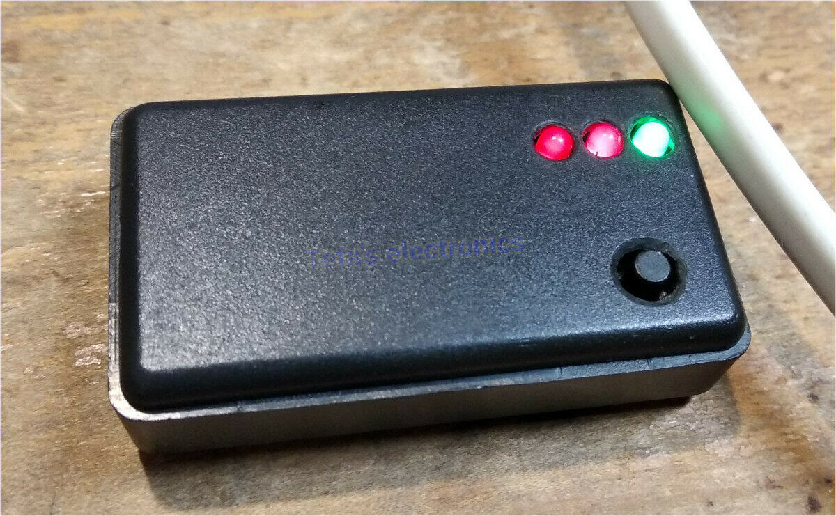
Simple live wire detector/finder (click for full resolution)

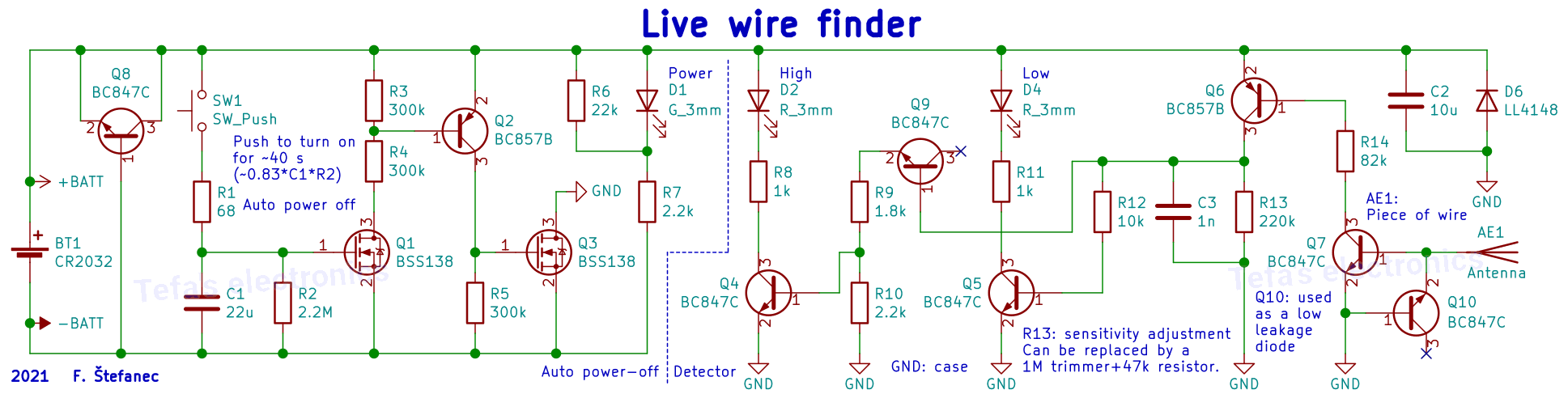
Simple live wire detector/finder - schematic diagram (click for full resolution)
This circuits consists of three transistors and a few other parts. It works as three amplifying stages connected together. If there is a live wire near the antenna, a small current will flow through the antenna due to capacitive coupling - if we assume 230 V, 50 Hz and a capacitance of 0.2 pF, the capacitive reactance is approx. 15.9 GΩ, allowing a current of around 14.4 nA (20 nA peak) to flow. If we neglect non-idealities of the parts and assume that each stage amplifies the current 100 times (the transistor amplifying factor depends on temperature, current, among other factors - so I chose this low estimate here), the output current should be able to fully light up the indication LED - 20 mA peak if there would be no resistor R3. Resistors R1-R3 limit the current flowing into the following stages and the LED.
The diode D1 protects the B-E junction of Q1 from excessive negative voltage/creates a conductive path during the negative half-wave. It there was no D1, the voltage swing would be about 8 V, as the B-E junction would go into breakdown in the negative half-wave. This would require higher currents to get such a voltage swing on the input capacitance (and wouldn't be good for the transistor).
If the circuit is too sensitive, a combination of a resistor with a value of a few tens to hundreds kΩ in series with a 500 kΩ trimpot can be connected between the base and emitter of Q3. This will allow the sensitivity to be adjusted.
In the prototype, transistors with the model name ending with "B" (gain about 300) were used - BC547B, BC557B. In place of R1, R2, 1 kΩ resistors were used. Part values aren't very critical.
Finished device, operating (click for full resolution)
Schematic diagram (click for full resolution)
This more complex version is powered by a single CR2032 cell, and is miniaturized.
The first part of the circuit (Auto power off) is used for power switching and timing. The transistor Q8 is used as a primitive ESD and reverse polarity protection. Pressing the switch SW1 allows the capacitor C1 to be charged through the resistor R1. After the switch is released, C1 slowly discharges through R2. As long as the voltage on C1 is higher than the threshold voltage of the MOSFET Q1 (BSS138), Q1 switches Q2 through R4 (R3 eliminates effects of leakage currents), which switches Q3 on. Q3 connects the negative battery contact to the GND node. The LED D1 signalizes operation, resistors R6, R7 set the current and minimum voltage for D1 (around 2.5 V is recommended - also used as low voltage indication). R2 and C1 set the time to turn-off after button release, in this case it is approx. 40 seconds. Three transistors are used here to get more gain - to limit the time where Q3 is partially switched on.
The detector itself works just like the simplified variant. Instead of the diode across the B-E junction of the first stage, the B-E junction of Q10 is used (in reverse). Its breakdown voltage is very low (which is not a problem here), but the leakage current is also very low. The first stage is followed by the second stage with Q6. R13 sets the sensitivity, in case it needs to be adjusted, it can be replaced by a series combination of a 10 kΩ resistor and a 500-1000 kΩ trimpot.
There are two indication levels, lower (LED D4) and higher (LED D2). The LED D4 is driven by Q5. If enough current flows into the base of Q5, D4 lights up, but some current also flows through the B-E junction of Q9 (it is used here instead of a typical diode like 1N4148 to get similar characteristics to the B-E junction of Q5). If the current flowing through the collector of Q6 (and also through Q9) is high enough to get a voltage drop of approx. 0.6 V on R10, the LED D2 will light up too.
The detector was constructed on an universal PCB using SMD parts and solderable enameled wire. The circuit board was then placed into a 50x28x15 mm enclosure. Residue visible on the PCB in some photos is just scratched colophony coating. The input stages are covered by hot melt glue (not a problem due to low operating temperature) to improve insulation - decrease the effects of leakage currents due to moisture. There should be no conductive residues on the PCB.
The antenna is built using copper tape glued to the bottom of the enclosure. Springy contacts (taken out of a USB connector) are mounted on the bottom of the circuit board. The copper tape is split into two parts, a shorter part covering the "front" and only a very small part of the bottom of the PCB (used as an antenna), and a large part covering most of the enclosure bottom, acting as a capacitive coupling between the GND node and ground/user. This is partially visible in the photos. The Cu tape is covered using insulating tape with cutouts for the contacts.

Top side of the circuit board (click for full resolution)

Bottom side of the circuit board (click for full resolution)

Insides of the enclosure (click for full resolution)
Warning, the detector can also detect voltages due to various capacitive couplings. It is only designed for detecting AC voltages. It is designed to be used for quick, rough measurements. If there is any risk of injury or property damage, another (and different) measuring method/tool should be used to complement this one. You do everything at your own risk.