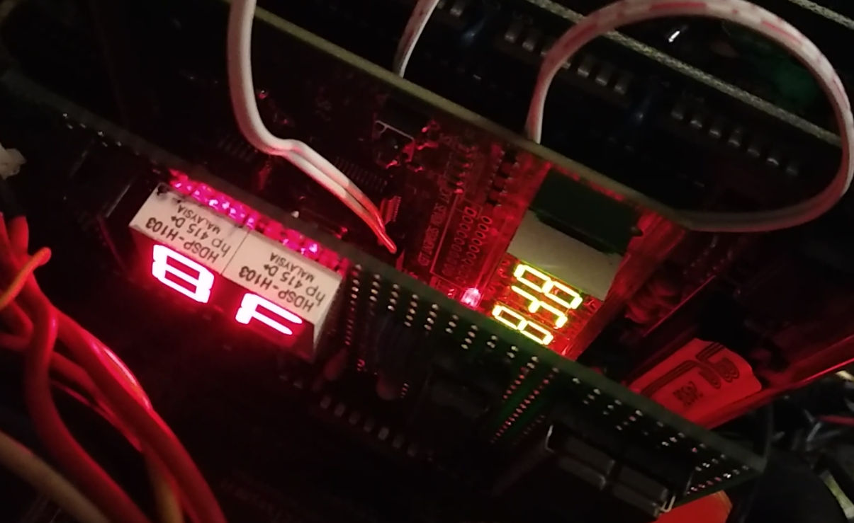
This is a diagnostic ("POST" - Power On Self Test) 8-bit ISA card used for debugging old motherboards with ISA slots. During the power of self test, the BIOS sends diagnostic codes to I/O port 80h. The card has a two digit hexadecimal display showing the last code sent to 80h. The codes may be different for different BIOS vendors and versions. In case a computer isn't starting properly and the graphics card won't initialize, so nothing is shown on the screen, a diagnostic card can be used to pinpoint causes of failure more precisely than beep codes. It is a very useful tool for debugging and repairing old/vintage (pre-2000) motherboards.
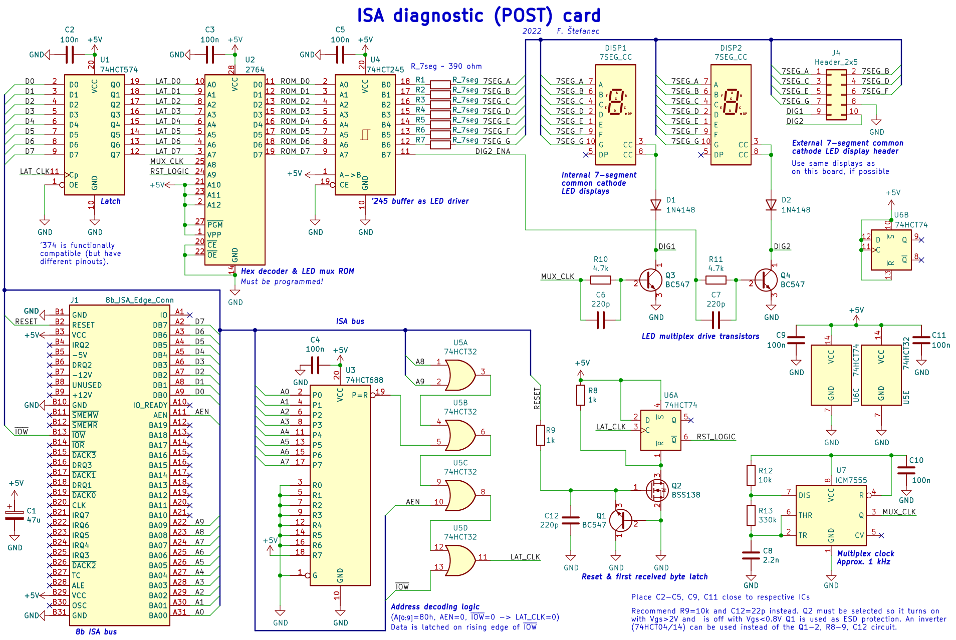
Circuit diagram (click for full resolution)
This card uses just the +5V power line. HCT, LS or ALS logic can be used. U3 (74HCT688) is a comparator which decodes the lower eight address lines and outputs a logical zero when A[7:0]=80h. OR logic gates (U5) are used to decode higher address lines (A8, A9 - the card decodes the lower 10 address lines), AEN (DMA vs CPU access) and ~IOW (I/O write command, active low). The card "listens" at the port 80h. When A[9:0]=80h, AEN=0 (bus controlled by the CPU, not DMA) and ~IOW=0 (writing to I/O), then the node LAT_CLK will be low, else it will be high. As ~IOW then gets deasserted (goes log. 1), while data is still present on the data lines (D[7:0]), LAT_CLK also switches from low to high. U1 (74HCT574 or '374 - equivalent function, different pinout) latches the data on the bus on the rising edge of LAT_CLK.
On reset, the flip-flop U6A (1/2 of 74HCT74) gets reset, setting its inverting output (RST_LOGIC) high. On any rising edge of LAT_CLK (any data received at 80h), U6A gets set and RST_LOGIC goes low. To invert the RESET signal from the ISA bus, as the reset inputs of 74HCT74 are active low, Q2 is used.
The hexadecimal code is displayed using two multiplexed common cathode 7-segment displays. The multiplex clock is generated using U7 (a 555 timer, normal or CMOS) and is approximately 1 kHz. The display anodes are driven using a 74HCT245 buffer (U4), the cathodes are driven using NPN transistors Q3 and Q4. Capacitors C6, C7 are used to speed up their turn-off. The '245 buffer can be flipped (A and B sides) if pin 1 is connected to GND instead. Decoding of hexadecimal data and multiplex control is done using a 2764 (U2, 27C64, e.g. NMC27C64Q or similar) ROM (a 27C256 ROM can be used as well, as long as pin 26 is connected to either +5V or GND). The ROM is programmed in such a way that the ROM pin D7 outputs the inverted value of the ROM A8 address input (MUX_CLK), which then drives the second digit mux switch, ROM pins D0-D6 output codes for the 7-segment displays (pins A-G) that correspond to inputs on either the ROM address lines A[7:4] (first digit, when MUX_CLK is high) or A[3:0] (second digit, when MUX_CLK is low). When the ROM input A9 (RST_LOGIC) is high, only "--" is displayed on the 7-segment displays, signaling that since reset, no code had been received yet.
1N4148 diodes are connected in series with the display cathodes, so that if the same or similar 7-segment displays are connected to J4, there isn't enough voltage to run the internal displays due to the ~0.7 V diode drop. Capacitors C2-C5, C9-C11 need to be close to the respective ICs. To protect the sensitive BSS138 MOSFET, a BC547 BJT B-E junction is used as a crude low-capacitance Zener diode (Q1 must be placed close to Q2). A single 74HCT04 or '14 gate can be used instead of this discrete inverter, and it would likely be a better solution. Alternatively, if a delay up to ~1 ms for recognizing ISA RESET going high is not a problem (in this case, it shouldn't be), U6B can be used (U6B ~S and D connected to +5V, ~R connected to bus RESET line, the C input connected to MUX_CLK, Q not connected, ~Q used as output, going to the ~R input of U6A, with R8-9, C12, Q1-2 not being installed at all).
The circuit is built on an universal ISA board, using solderable enameled wire and mostly THT components. A protective coating of shellac+resin is used to protect the finished card.
The ROM needs to be programmed. A TL866II+ programmer was used. Binary files are available for download at the end of this page. Only 1 kB of the ROM is used (first 10 address lines, the data is just repeated), and the circuit can be modified for other ROMs.
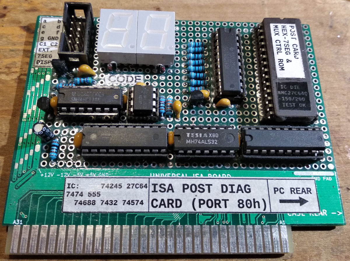
Prototype, top (click for full resolution)

Prototype, bottom (click for full resolution)
Pin 8 of U7 (ICM7555) and parts C10, R12 should be connected to the +5V rail, but the connection is missing in the schematic. Without this connection, the display will not work properly.