DISCLAIMER! Dangerous voltages are present inside this device. You do everything at your own risk.

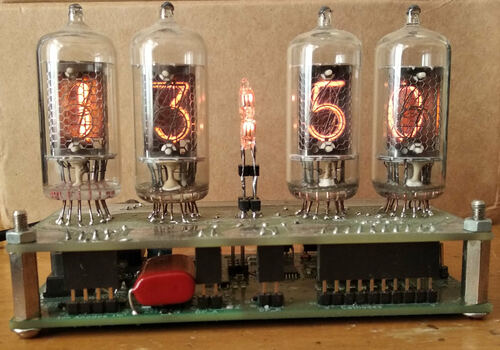
Operating (click for full resolution)

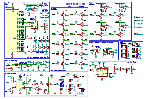
MCU board schematic diagram (click for full resolution)
The main circuit boards consists of several parts:
The +180 volt power supply is a classic step-up (boost) converter based on the MC34063 integrated circuit. It is operating in discontinuous mode. Peak current is set using R1 (0.22 Ω in diagram, later increased to 0.47 Ω). The MOSFET Q2 switches the inductor L1, when it's switched off, the stored energy is then discharged through D6 into C8 and a filtering film 1 µF capacitor (attached to J10, J11). Parts R3, D2, R4, Q1 drive the MOSFET. R2 limits current, R3 and Q1 discharge the MOSFET gate, D2 bypasses Q1 when charging the gate. Output voltage is set using R12, R13, RV1. RV1 can be used to accurately adjust the output voltage. R16, D7 shut down the converter until the MCU pulls down the HV_INHIBIT node.
Nixie cathodes are driven using Q3-Q7, Q10-Q14. Anodes are driven using Q16-Q23. Nixie tube current is limited using R17 (10 kΩ 2 W) to approx. 4 mA (the nixie voltage drop is around 140 V when on), therefore 1 mA per nixie on average (they are multiplexed). The colon is implemented using two neon glow tubes (NE-2H) and is driven using Q8, Q15 and the current is limited by R40, R41 to around 250 µA (assuming 80 V drop). All outputs go to a separate board through J3-J6 (long pin headers). Such pin headers are designed for low voltages, but used anyway.
The MCU (U1: ATtiny88) is powered using the +5 V rail. It runs at 8 MHz using its internal oscillator. It is used to control the cathode/anode drivers. Anode multiplex is combined with button multiplex (nodes DRV_A-DRV_D). Parts R8, C11 filter the signal coming from the button multiplex circuit. To prevent excessive losses in the HV supply if the input voltage is too low, undervoltage lockout is implemented using the MCU's ADC, firmware, voltage divider formed using R25, R42 and pin PB1 controlling the "HV_INHIBIT" node. The user interface is described below. Some features (external clock input J8, speaker output J7) are not implemented yet. The MCU and RTC communicate using I2C, which is broken out using J9 for possible upgrades, debugging etc.
The RTC (Real Time Clock) is based on U4 (DS3231MZ). Battery backup is available (BT1). This IC has better than ±5 ppm default accuracy (approx. 0.4 seconds per day), which can be further improved. The PCB layout was made in a way where the battery holder was supposed to be installed on the PCB back side, but in the end it was placed on the same side as other components, with small rubber standoffs preventing it from touching other components.
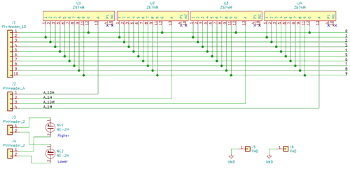
All of the Nixie tubes and neon lamps are placed on a separate board.

Nixie board schematic diagram (click for full resolution)
There are only few parts on this circuit board. However, to prevent or decrease display ghosting, it might be necessary to install resistors (approximately 2.2 to 4.7 MΩ) between each anode line (A_10H, A_1H, A_10M, A_1M) and GND. A combination of Z570M and Z574M tubes is used, either type can be used - it is recommended to stick to one type. The tubes used here had their red coating already damaged, so it was fully removed. Warning: there is some issue with ghosting that wasn't solved yet.
14 mm standoffs are used between the boards.
There are 4 buttons, DRV_A (leftmost when looking at the clock from the nixie back side) corresponds to "back" in settings, next button function is "forward", followed by "decrease" and "increase". Going forward will allow the user to set hours, minutes, seconds, year, month, day in this order. The date is in DD.MM format. In settings mode, the colon does not blink. When nothing is changed, nothing will be saved (e.g. the time will not "stay stuck" when in the settings mode), so it's possible to view seconds and date without holding the clock back.
To calibrate the clock, when all 4 buttons are held during power-up, calibration mode will be entered. In this mode, the aging offset of the DS3231M can be set. After entering this mode, "9999" blinks on the nixies for several seconds before any adjustment is possible. Upper neon lamp of the colon denotes positive value, lower lamp denotes negative value. The value can be adjusted between -127 and +127. Each LSb corresponds to a change in frequency of approximately 0.12 ppm, according to the DS3231M datasheet. Pressing the "forward" button 5 times saves the value into both the DS3231M IC and the ATtiny EEPROM. This is signalized by "9999" for a few seconds, before entering normal operation mode again.
In normal operation, the clock displays hours and minutes, the colon blinks once a second.
Additional functionality such as alarm might be eventually implemented.
The firmware is written in C using Code::Blocks. AVR fuses are: EFUSE: 0xFF; HFUSE: 0xDC; LFUSE: 0xEE. The avrdude command is:
avrdude -c usbasp -p t88 -U flash:w:'<path>Tiny88_NixieClock.hex' -U hfuse:w:0xdc:m -U lfuse:w:0xee:m
The HEX file and source code is included in downloads.