WARNING! Lithium-ion batteries should be handled with care. Violent chemical reaction can occur when the battery is damaged. Don't overcharge, overload, short-circuit, underdischarge or mechanically damage Li-ion batteries.
This power bank kit was bought on AliExpress for approximately 2 USD. It takes 3 regular 18650 3.6/3.7 volt Lithium-ion cells.
The following text is printed on the case:
Input: 5V±5%= 1A Output: 5V±5%= 2.1A
Capacity: 8400mAh Made in China
Board markings: YDJ-202-V1.0 1502-0706

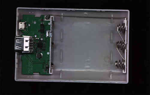
Inside (click for full resolution)

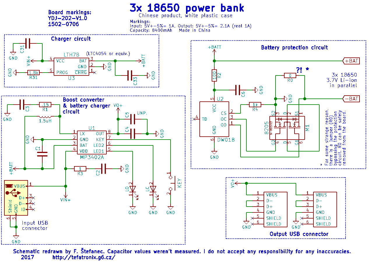
Reverse engineered circuit diagram (click for full resolution)
This is a regular cheap power bank kit. You have to add your own batteries. All three cells are connected in parallel.
This power bank is based on the MP3402A chip (U1) by Thinkplus Semiconductor. This chip integrates a battery charger, protection circuitry and a synchronous boost converter in a single 8-pin SMD package. These chips (MP3401A, etc...) are very common in inexpensive power banks. Only few external parts are required. There are a few resistors and capacitors, an inductor, a push button and two LEDs connected to the MP3402A.
There is also an additional dedicated Li-ion charger IC, marked LTH7B. This is likely an LTC4054 or some clone/equivalent. Its charging current is set by the resistor R31 to approximately 500 mA. The total charging current is 1250 mA (measured).
There is also a battery protection circuit, based on the DW01B chip, probably manufactured by Fortune Semiconductor. Together with the MOSFET M1 (marked 8205), this forms an overcharge, overload and underdischarge protection for the battery. For some strange reason this circuit was bypassed by a zero ohm resistor/jumper (R0). (!!!) It makes no sense to include a protection circuit and then disable it. Removing R0 had no adverse effect on the power bank's functionality.
A micro USB connector is used for charging. There's a double USB output connector. However, the total maximum current this device can supply is still around 1 A, so it won't be able to charge any two more demanding devices at once. It doesn't meet its specifications (able to output only around 1 A, while specified to 2.1 A).