DISCLAIMER! High voltages are present in this device, strong electromagnetic fields are emitted during operation. The device should NEVER be run without proper shielding. The high frequency high voltage output isn't likely to kill or seriously harm a healthy person, although it can cause painful burns. It's very dangerous to people with pacemakers or any similar devices. I refuse to take ANY responsibility for any possible injuries, legal problems (these might arise due to the interference this device produces), property damage or deaths, anything you find here is provided WITHOUT ANY WARRANTY and you do everything AT YOUR VERY OWN RISK!

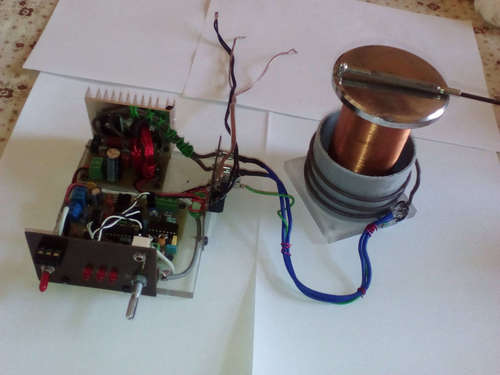
Finished device: (click for full resolution)
I am not going to discuss the basics/operation principles of Tesla coils here, for that, check out this article [insert link here]
This is my first properly working solid state (semiconductor-driven) Tesla coil. It's based on the 74HC4046 PLL IC and uses the VCO from it. I have used the powerful UCC37322 gate driver, but it also works with the cheaper and more available TC4420. The circuitry is separated to two circuit boards, one for the control circuitry, containing a voltage regulator to provide stable 5 volts to the logic circuitry, the 74HC4046 chip and auxiliary logic circuitry (a 74HC08 quad 2-input AND gate and a 74HC14 hex schmitt-triggered inverter). The power circuit board contains the switching transistor (an IRFP260, which is a 200 volt, 50 ampere (200 peak) MOSFET), power diodes and connectors for the primary and energy recovery coils.

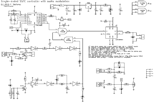
Controller board schematic (click for full resolution)
In the top left part, we can see the oscillator (parts U1, R1, R2, C1, C2). The frequency can be changed by changing the capacitance of C1, C2, I use 470 pF for both capacitors, which works OK for my coil. The 74HC4046 chip can also function as a phase locked loop, this can be enabled by enabling JP1. Feedback is then connected to P3 and clamped through the diodes D1, D2 to ground/5V, preventing damage to the 74HC4046. A small antenna can be used for feedback, using feedback will make the coil harder to go out of tune. The output of the oscillator is connected through U3A to the gatedriver, which is able to sink/source large currents in order to charge/discharge the power MOSFET's gate.
The undervoltage lockout circuitry consists of R3, R6, R7 as the voltage divider, C4 for noise spression, U2D-U2F to invert the signal, clean up noise and add an additional delay with the help of D4, R19, R11 and C6. The LED diode D7 signalizes that the power is good and the device is operating.
The device can be ran in both continuous and interrupted mode. The interrupter can be connected to P1. Pin 1 acts as a 5V power output, pin 2 is the device's input (output of the interrupter) and pin 3 is connected to ground. The input should accept TTL signals and tolerate voltages up to about 15 V. A switch is connected to P2, when it's closed, the device will operate in CW - continuous wave- mode. D6 signalizes that the device is operating (either the CW switch is on or the interrupter output is HIGH). The interrupt signal and the power good signals are combined through an AND gate (U3B), which has the output connected to one input of U3A. If the signal there is LOW, the device is off (gatedriver output is LOW).
Audio modulation of the sparks is possible by detuning the coil by an audio signal AC-coupled to the VCO input (through C10). Audio input can be connected to P5. A tuning potentiometer (around 5-50 kΩ, I use 10k) can be connected to P6, making it easier to retune the circuit
The gate signal is present at P7, pin 1 should be connected to the gate and pin 2 to the source of the power MOSFET. A twisted-pair cable should be used for this purpose.
The connector P4 is used as power input, with pin 1 being the + input and pin 2 being the ground. This is then fused using F1, filtered using C5, C7, protected against bad polarity using D5 (a 15V Zener diode would be better though) and used to power the gatedriver. The 5V voltage is stabilized using U4 and C8. Capacitors C12, C13, C14, C15 are used for decoupling/blocking and must be close to the respective logic ICs.

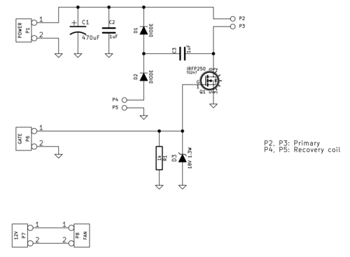
Power board schematic (click for full resolution)
The 0-24 volt input is connected to P1, + to pin 1 and ground to pin 2. The primary coil is connected to P2, P3, the recovery coil (here I have used an air coil with 22 turns on 3cm diameter, with an inductance of around 20 microhenries) is connected to P4, P5. Its function, together with D1 and D2 (fast power diodes, I have used BYW29-200), is to "recover" the spikes that are created when Q1 is turned off, limiting the voltage there to approximately twice the input voltage by returning the unused energy back to the filtering capacity (C1, C2), preventing the MOSFET from overheating or getting destroyed by spikes. P2-P5 are faston type connectors.
The gate signal is connected to P6, with pin 1 being the gate input and pin 2 connected to source/common ground. R1 and D3 are there to protect the gate from voltage spikes.
Some heat is generated during operation and has to be properly dissipated, so a heatsink is required (Q1, D1 and D2 must be mounted on the heatsink, I have used the heatsing from an old graphics card. It can keep the device cool when operating from 12 volt power, but for 24 volts, the heatsink gets very hot and a cooling fan is required, and can be connected to P8, with P7 then being the power input for the fan.
Capacitors C1, C2 must be good quality, non-polarized, preferably foil capacitors for pulse operation, they are subjected to currents in excess of 10 amperes. Electrolytic capacitors CAN NOT be used.
The secondary coil is wound on a 5 cm diameter, approximately 10 cm long piece of PP plastic waste pipe (bought in a local hardware store) using enameled 0.15 mm wire. The total winding height is about 9 cm and may contain around 550 turns. Resonant frequency is in the ballpark of 1.2-1.5 MHz depending on the used breakout point (I use a nail) and the coil's surroundings.
The primary coil is wound on a 7 cm diameter piece of a plastic pipe, and consists of 3 turns of 1.5 mm2 wire. The winding height is something around 2 cm.
ZIP archive - circuit board files (600 DPI bottom side patterns, KiCad files).