DISCLAIMER! High voltages are present in this device, strong electromagnetic fields are emitted during operation. The high frequency high voltage output isn't likely to kill or seriously harm a healthy person, although it can cause painful burns. It's extremely dangerous to people with pacemakers or any similar devices. I refuse to take ANY responsibility for any possible injuries, legal problems, property damage or deaths, anything you find here is provided WITHOUT ANY WARRANTY and you do everything AT YOUR VERY OWN RISK!
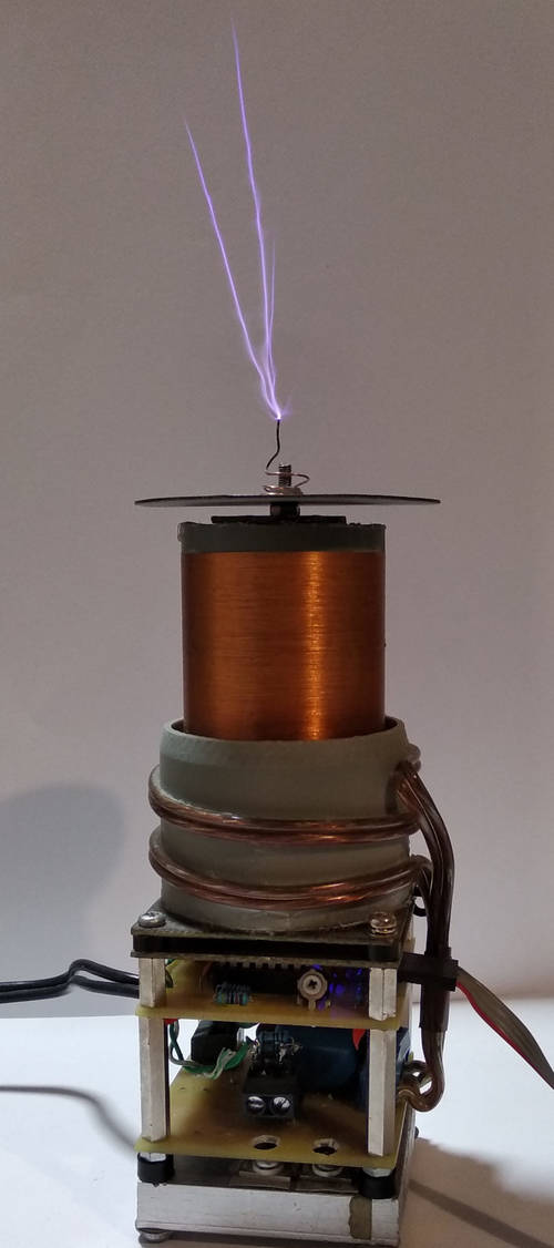
Finished device - running at approx. 30 volts (click for full resolution)
This is a small solid state Tesla coil capable of running at very low input voltages.
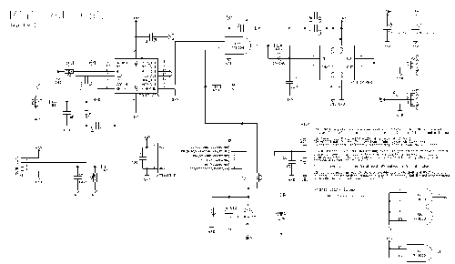
Controller board schematic (click for full resolution)
In the top left part, we can see the oscillator (parts U1, R2, R3, C3). The frequency can be changed by changing the capacitance of C3 and/or the resistors R2, R3, here I use 1 nF, 10 kΩ, 10 kΩ. You will find the exact formula to calculate the values in the 74HC4046's datasheet, or there are some online calculators (search for "74HC4046 frequency calculator"). The frequency can be adjusted (coarse adjustment) using the trimpot RV1. Pin 3 of P1 is used for fine tuning. The phase-locked-loop functions of the 74HC4046 chip are not used. The output of the oscillator is connected through the logic gate U3A (which "mixes" the oscillator signal and the interrupter signal, both must be log. 1 for the output to be log. 1) to the gate driver, which then drives the MOSFET on the power board. I use a UCC37322 as the gate driver (which also means the 74HC08 IC is unneccessary in this device, however, it's there so other gate drivers with no ENABLE input can be used too - such as TC4420, TC4422, TC4452...). Decoupling capacitors (C11 and C10) MUST be installed as close to the gate driver chip as possible (to minimize stray inductance). I use 0805 SMD capacitors mounted on the underside of the circuit board. They should be of good quality (preferably no electrolytics - equivalent serial resistance and inductance must be as low as possible). Bad quality capacitors or high stray inductance will lead to ringing, bad performance and potential damage to components.
The undervoltage lock-out (UVLO) and interrupter duty cycle limiter functions are implemented on an ATtiny13-P microcontroller with only few external parts. The interrupter signal is connected to pin 2 of P1. R12 and C12 are there to "average" the output signal of the MCU (this isn't perfectly accurate, but good enough for protection purposes). The duty cycle limiter can be disabled by installing JP1. R11 can be left unpopulated, originally it was there for some testing purposes. The resistors R9, R8 form a voltage divider for UVLO. The voltages from the duty limiter low-pass filter (R12, C12) and the power voltage divider (R9, R8, C10) are read using the ATtiny's integrated ADC (pins PB2 and PB4) and compared with pre-programmed values. In case they exceed the set limits, the ATtiny disables the output (pin PB0). The LED (D1) is there to signalize the status of the protection circuit. If it's constantly lit, everything is OK. If it's blinking, something's wrong (there are different blinking patterns for "too low voltage" and "duty cycle exceeded"). The device goes back into normal operation shortly after the error condition is corrected. The MCU is running at 9.6 MHz, using the integrated RC oscillator. The firmware is written in assembly language (.asm and .hex files are available at the end of this page). Thresholds and blink patterns can be modified by editing the firmware. I tried to keep the delay introduced in the interrupter signal (by the microcontroller) as low as possible, in this case it's not more than 3 µs. The microcontroller has to be programmed, otherwise the device won't work. When programming, the high fuse should be set to 0xF9 and the low fuse to 0x7A.
The high-frequency output duty cycle (not interrupter duty cycle) should be under 50%, so it's limited a bit by the resistor R13, diode D2 and capacitor C13. In my device, I use 470 Ω and 100 pF. This makes the rising edge of the signal slower than the falling edge. Together with the Schmitt trigger function of the input of the gatedriver, this decreases the duty cycle. The output signal of the gate driver is connected to P2 and connected to the power board through a short (as short as possible) piece of cable consisting of two twisted wires, with a 4.7 ohm resistor connected in the "gate" signal.
The power input is connected to P3. A small feritte core is installed on the 3-wire cable to limit common mode noise/interference.
All decoupling capacitors - C5, C6, C8, C10, C11 - have to be installed as close as possible to the respective integrated circuits.
The device is designed to be used with an interrupter. The interrupter should be connected to P1 and is also described on this page.
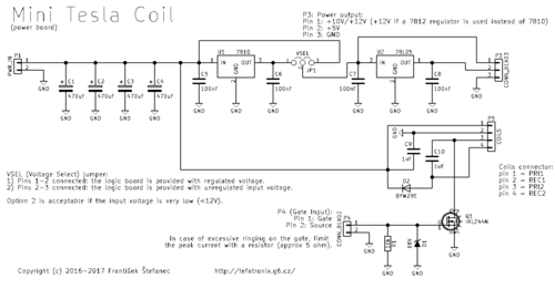
Power board schematic (click for full resolution)
The final stage is single-ended, with a single MOSFET, similar to Danyk's ISSTC 3 (link here)
The 8-19 volt input is connected to P1, + to pin 1 and ground to pin 2.
The gate drive signal is connected to P4, with pin 1 being the gate input and pin 2 connected to source/ground. R1 and D1 are there to protect the gate from voltage spikes.
The secondary coil is approximately 6.5 cm high and has around 600 turns of 0.1 mm diameter wire wound on a 4 cm diameter pipe. Its other end (opposite to the high voltage output) should be grounded. Resonant frequency calculated using Rayer's online TC calculator is 1.39 MHz, which is close to the measured 1.45 MHz.
The primary coil has 2 turns of 1.5 mm2 speaker cable wound on a 5 cm diameter pipe. There is also an energy recovery coil. These two coils have to be physically close to each other, the closer the better - coupling should be as close to k=1 as possible. These two coils are wound at once, using a 2-wire speaker cable. The coupling between the primary and secondary coils is around 0.3 or so (guesstimation).
Capacitors C9, C10 have to be of good quality, preferably foil capacitors for pulse operation, they should be able to withstand several amperes. Don't use electrolytic capacitors. I use some epoxy dipped, 250V-rated capacitors (not sure about the model) and they seem to work fine so far.
The primary coil is connected to P5, pins 1 and 3. The recovery coil is connected to P5 pins 2 and 4. Proper phasing is crucial for proper operation of the device. Both coil "winding beginnings" (or both "ends") have to be connected to pins 1 and 2.
The energy recovery circuit consists of D2, C9 and C10. The capacitors are there for power decoupling and to make up for possible imperfections of the magnetic coupling. They act almost like a short circuit for fast changing AC currents (reactance: XC=1/(2*π*f*C)=1/(6,28*1450000*1µ)=approx. 100 mΩ) and are almost open for DC currents. Working principle (with supply voltage 12 V):
There is a jumper marked "VSEL". Pins 1-2 should be connected together to supply the logic board (its power input is connected to P3) with regulated voltage (10 V from the voltage regulator (7810) - I used a 12V stabilizer instead of a 10V one, but that doesn't change the working principle). Connecting pins 2-3 together will supply the logic board directly with the supply voltage from P1 - recommended and safe ONLY with input voltages below 10-12 V, where this is necessary.
The MOSFET and recovery diode have to be heatsinked! Be careful, as their cooling tabs are not electrically isolated. I use a 1 cm thick, 5x5 cm plate as both the heatsink and the base of the entire device.
The decoupling capacitors (C5-C8) have to be close to the voltage regulators (U1, U2). The power decoupling/DC blocking capacitors, MOSFET Q1, diode D2 also have to be physically close to each other. Keep all wiring as short as possible.
The IRLZ44N MOSFET used here isn't suitable for higher powers - however, it's good for very low input voltages. For higher power, use a more powerful MOSFET - such as SUP85N10.
The bottom end of the secondary coil has to be properly grounded!
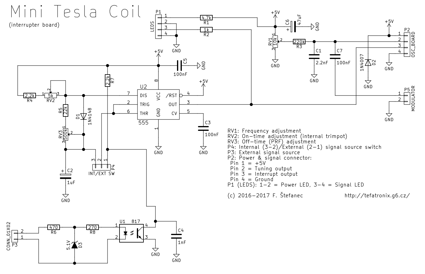
Interrupter schematic (click for full resolution)
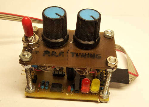
Interrupter (click for full resolution)
This is the interrupter board circuit. It's connected to the logic board. P2 goes to P1 on the controller board. The pins are numbered backwards here. (Pin 1=VCC, pin 2=tuning, pin 3=interrupt signal, pin 4=GND).
There is a potentiometer (RV1) for fine tuning of the high frequency oscillator on the main board.
This circuit is based on the well known 555 timer and designed to generate short pulses with a certain pulse repetition frequency. The pulse width is set by adjusting RV2 (small trimpot on the board) and the PRF is set by adjusting RV3 (normal potentiometer). All wiring to the potentiometers should be as short as possible.
There is an external optocoupled input (P3). To generate the pulses "locally", pins 3 and 2 of P4 are connected together, to use the external input, pins 1 and 2 of P4 are connected together. A switch can be installed there (keep wiring short!)
Two LEDs are connected to P1, power indicator LED to pins 1 (A) and 2 (K), signal LED to pins 3 and 4.
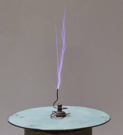
Sparks at 19 V in (click for full resolution)
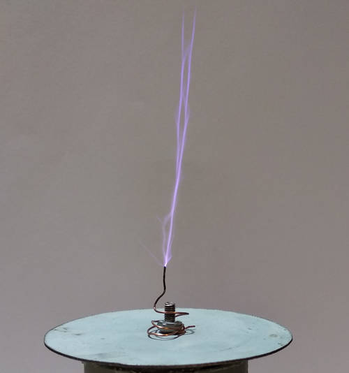
Sparks at 19 V in (click for full resolution)
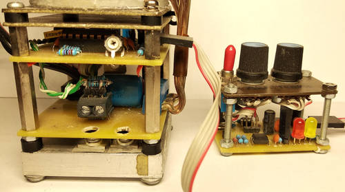
Internals (click for full resolution)
To achieve higher spark length, I replaced the power MOSFET and diode with SUP85N10 and MUR1560 and replaced the gate resistor with a 2.2 ohm one, installed a fast diode parallel to it (anode to gate), and also installed a miniature ferrite bead on the gate signal wire. Because the SUP85N10 MOSFET has around 5 nF gate capacitance, I had more problems with ringing. With these parts, it's possible to get sparks longer than the secondary coil itself - longest measured sparks to air were longer than 8 cm. For this combination, the driver voltage should be 12 V (use a 7812 regulator) & the UVLO level should be set to around 10 volts.
Better cooling is required at such power levels - I managed to fry several MOSFETs. Now I have an IRF3205 in place (temporarily) - it's quite slow (and its VDS rating is too low). At 32 V input voltage, sparks (into a grounded object) as long as 10 cm can be achieved.
Another big problem arises when the logic board is too close to the coils - the magnetic field will interfere with its operation. For this reason, there are standoffs and a piece of PCB material (unetched, just a copper coated board) under the coils, protecting the logic board.
It's recommended to add a small topload to decrease resonant frequency.