DISCLAIMER! High voltage experiments are dangerous. I refuse to take ANY responsibility for any possible injuries, legal problems, property damage or deaths, anything you find here is provided WITHOUT ANY WARRANTY. Tesla coils also create considerable electromagnetic interference. You do everything AT YOUR VERY OWN RISK!
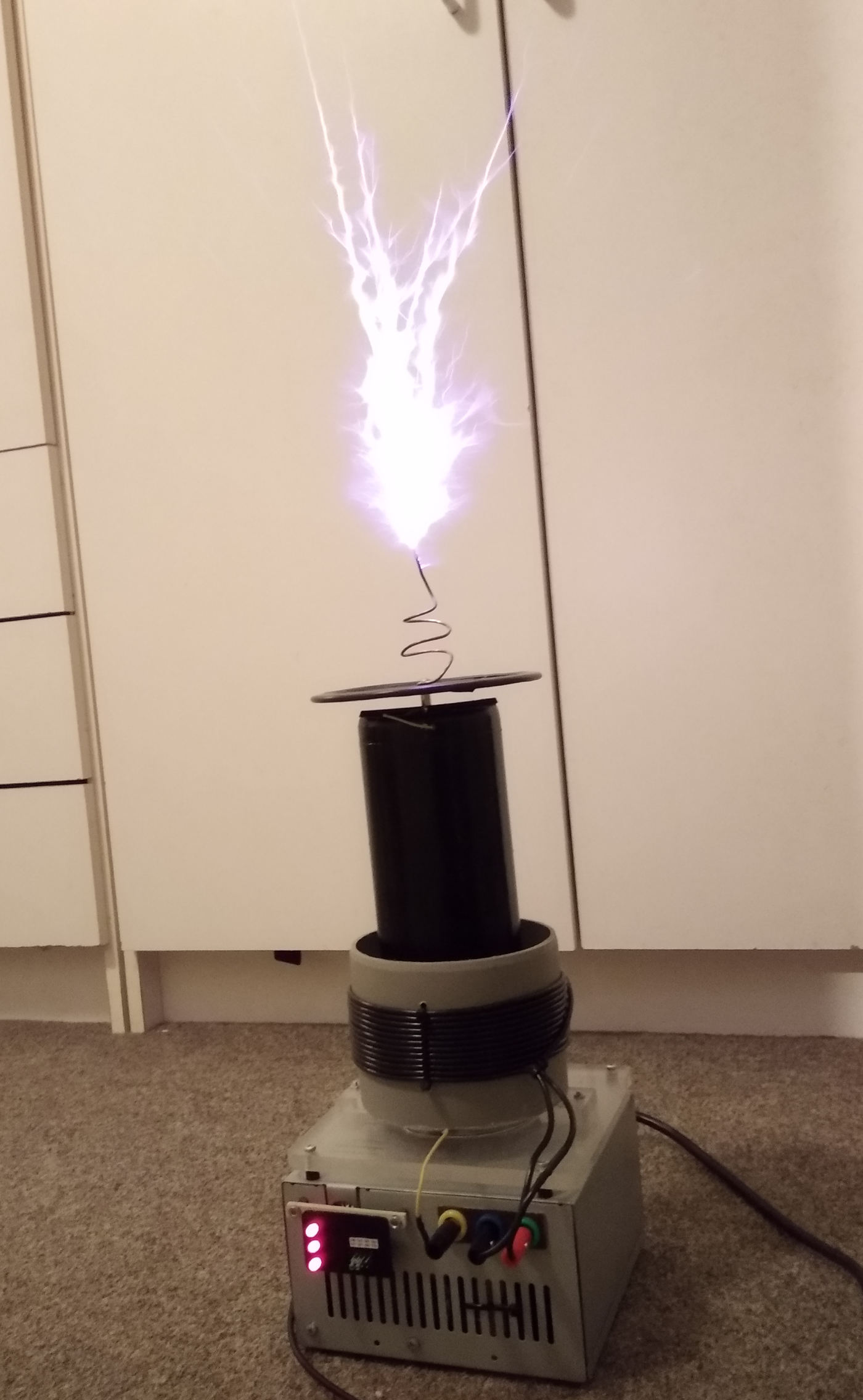
Finished device (click for full resolution)
After building several small solid state Tesla coils, I wanted to build something slightly bigger. This SSTC is based on a full bridge of IRFP460N MOSFETs driven with a PLL driver (robust, can withstand drawing arcs, etc.) without damage.
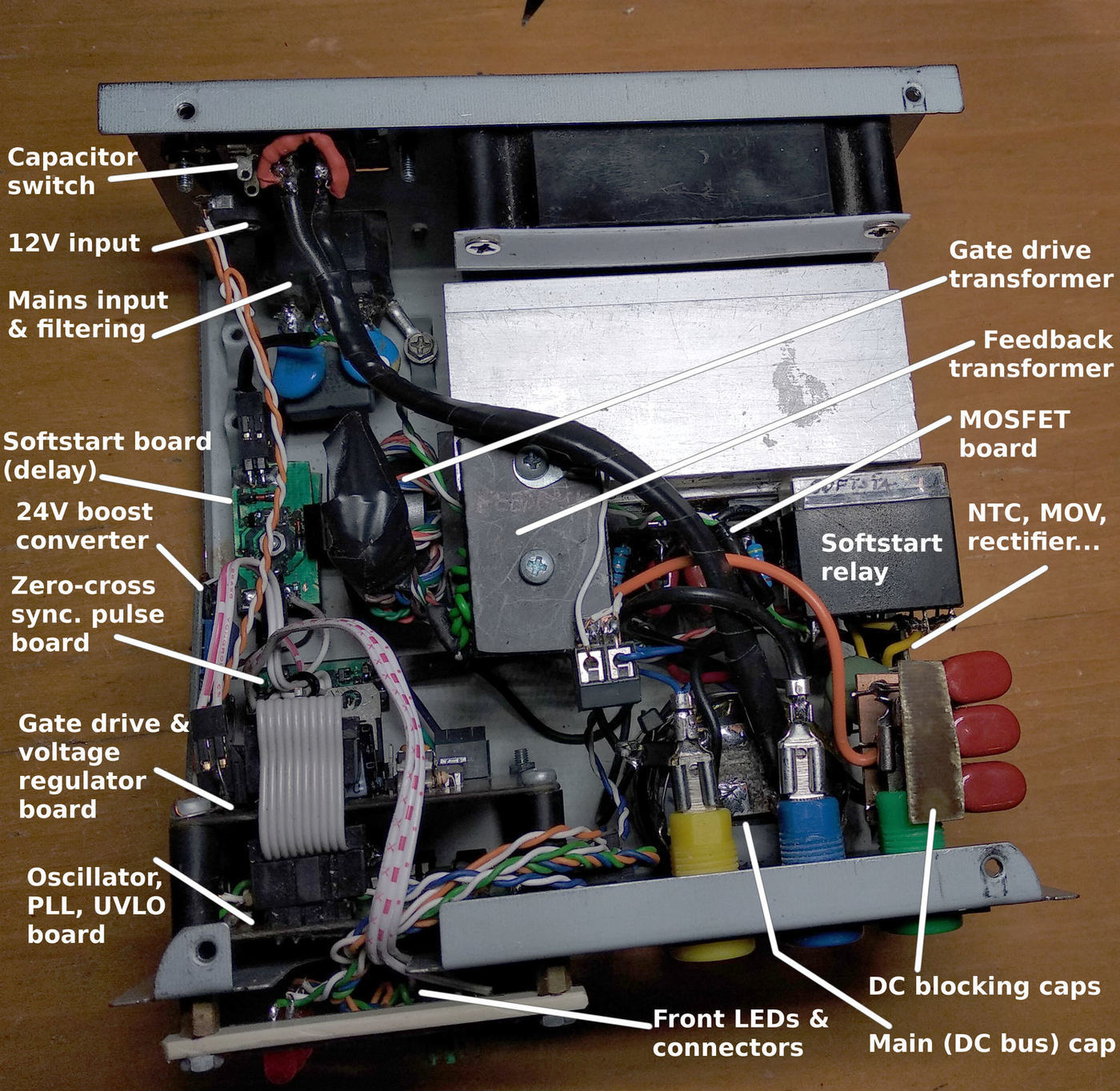
Inside (click for full resolution)
The circuitry is split onto several circuit boards: PLL board (oscillator, feedback, PLL, UVLO...), gate drive+voltage regulator board (containing gate drivers driving four small MOSFETs, which then drive the main bridge), zero-cross sync pulse generator, NTC+MOV+rectifier board. The gate drive/voltage regulator and PLL boards are connected with a 10 conductor flat cable.
The circuit boards are housed inside an old ATX power supply case. The coils are mounted on a piece of acrylic, which is then mounted onto the case.
I started working on this project quite a long time ago, the circuit diagrams may not be 100% accurate. Replicate at your own risk.
The secondary coil winding is 20 cm tall and is wound on a 7.5 cm diameter PP pipe. It's wound using 0.15 mm diameter enameled wire and covered with black acrylic paint. A circular piece of metal (12 cm diameter) is used as a topload/additional capacitance. The coil resonates at ~350 kHz.
The primary coil winding is about 4 cm tall and is wound on a 11 cm diameter pipe. It has 12 turns. The inductance is approximately 20 µH.
Both coils are mounted on a detachable plexiglass/acrylic plate.
The coils are connected to the base with banana plugs. Isolated (safety) banana plugs should be used. In the first photo normal uninsulated banana plugs are used, this was only a temporary solution (it's a considerable safety hazard).

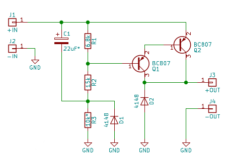
Gate driver board schematic (click for full resolution)
This circuit board contains 2 voltage regulators. Predriver voltage can be adjusted with RV1 - should be adjusted for good gate waveform while maintaining reasonable power consumption. The MOSFET gate driver consists of a "predriver" stage based on two TC4421 gate drivers, which then drive some smaller MOSFETs. I used IRFD024/IRFD9024 (DIP packages) because I had them on hand, but I recommend choosing different packages (the power dissipation isn't negligible). The gate driver idea was taken from Steve Ward's Universal DRSSTC driver. This board is connected to the PLL board using J4.

PLL board schematic (click for full resolution)
Parts D1, R1, R2, R3, R7, Q1, D4, C2 and U1A form the UVLO/power good detection circuit. If the voltage is lower than approx. 11 volts, the device won't operate.
The oscillator/PLL circuit is based on some work from a user nicknamed Wolfram (at 4hv.org). It is based on the 74HC4046 IC. Operating frequency is in the range of 250-350 kHz and can be adjusted by changing C1 and Ext_Cap1 (lower capacitance = higher frequency). The phase comparator consists of the following parts: U4B, XOR gate from U3 (PC1OUT), U1E, U1D and U5D. It compares the delayed (delay is added to compensate for delays induced by gate drive & MOSFETs) oscillator signal to the feedback signal. In case of a phase difference, the frequency gets turned up/down (U4B detects which signal comes first, U1E+U1D form delay compensation (adjustable with RV1). During the time when the signals are different, the XOR output of U3 switches U5D on. The resulting signal is filtered with a low-pass filter formed by R15, C5 (3.3 kΩ, 4.7 nF seems to work well for the used frequency range) and adjusts the VCO frequency. Start-up frequency can be set using RV2.
The feedback signal from the current transformer (connected to J1 - approx. 1:30 turns on a suitable ferrite core, sensing current through the secondary coil's bottom wire (earthed)) is clamped and reshaped using R21, C10, R6, D2, D3, D5, D8, R22, U1B. A 180° phase shift can be selected with J6 (the PLL will stay at one end of the frequency range when it's set to the wrong position).
An interrupter can be connected to J2. An additional overcurrent detection circuit can be connected to J3. If both outputs are high, the output of U2C (AND gate) is also high. This interrupter signal is synchronized to the oscillator signal using U4A.
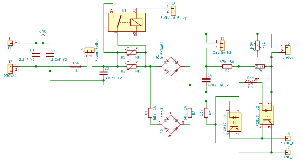
Mains input, MOSFET bridge (click for full resolution)
There are some filtering capacitors on the input, a fuse, NTC (coming from a power supply, with several ohms "cold" resistance), relay to bypass the NTC (driven by a circuit described below), a full bridge rectifier, optocouplers for zero-crossing and "big capacitor" detection. The main filtering capacitor (C4) can be connected/disconnected using a switch connected to J5 (this switch should not be manipulated with while the device is on, it has to also be able to withstand large currents). A 1 MΩ resistor is also connected in parallel to R3 in the finished device. J6 is the DC output that goes to the bridge. The MOV is a typical 275 VAC/370 VDC MOV.
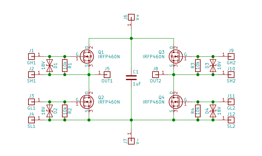
Bridge (click for full resolution)

GDT wiring (click for full resolution)
The bridge consists of 4 IRFP460N MOSFETs. The circuit board layout is crucial, inductances should be as small as possible. 3 capacitors (1 µF 400 V polypropylene) in parallel were eventually used in the place of C1. The primary coil is connected to J5, J8 through a DC blocking capacitor (3x 1 µF 400 V polypropylene capacitors connected in parallel together with a 330 kΩ resistor - the reactance (XC=1/(2*π*f*C)) is 143 mΩ, which is much lower than the reactance of the primary coil). The capacitors have to be able to withstand large currents! The MOSFETs are driven through a gate drive transformer. It is wound using UTP cable, using 4 conductors as the primary and the remaining 4 as secondaries. High permeability ferrite material should be used and shouldn't be driven near saturation.
The MOSFETs dissipate quite a lot of power. Considering that the primary inductance is 20 µH, at 320 volts (square wave) the peak magnetizing will be Ipeak=V/(4*f*L), approximately 11.4 A. It reaches its peak at the time the MOSFETs are switching. Considering the MOSFETs have a typical rise time of 87 ns and a fall time of 33 ns (ignoring non-ideal gate drive and any effects of the secondary coil), the bridge's switching loss will be around 77 watts (PSW=0.5*Vbridge*ISW*(tr+tf)*fsw), this loss is distributed across all MOSFETs (two MOSFETs sharing the load (same current, 1/2 voltage), two and two MOSFETs switching alternately). To approximate the conduction loss, I assumed the primary current to be a sine wave (the primary current resembles a sine wave, the current was measured to be around 15 A peak (approx. 11 A RMS) - it consists of the magnetizing (triangular) current and a sine wave that's mostly in phase with the output current, therefore I neglected it in switching loss calculations). The MOSFETs have a higher resistance when heated (approx. 0.4 Ω per MOSFET at 75°C instead of 0.24), two MOSFETs conduct at a time, practically in series. Therefore the conduction loss is approx. 0.8*112=97 watts. The total dissipated power by the bridge is around 174 watts according to this estimation (diode and output capacitance loss was neglected). A fairly big CPU heatsink is used here, together with a powerful fan, however I'd advise using a much bigger heatsink for long operation in filtered CW mode. In interrupted, unfiltered CW or ramped modes, the average power dissipation will be much lower. Even in CW mode, the dissipation will be lower (470 µF is not large enough for several kW power draw). Kapton insulating pads are used. The main bridge rectifier also has to be heatsinked. It is a good idea to also connect some very fast diodes (rated at least 10A, 600V) in parallel to the MOSFETs' body diodes. Adding transient voltage suppresors between drains and sources is also a good idea. A thermal protection circuit will be eventually added. In practice, I found out that during normal operation, the bridge doesn't get excessively hot. The MOSFETs' maximum junction to case thermal resistance is 0.45 °C/W, at 43 watts per MOSFET, the junction will be around 20°C hotter than the case. I don't recommend going over 100°C. (TJ(max) is 150°C according to the datasheet, but the switching times, resistance and other parameters get worse with high temperatures). Thermal pads also add some thermal resistance - around 0.2°C/W for thin kapton pads.
Some deadtime is added by the diode+resistor circuits (faster discharge, slower charge) shown in the second schematic. GDT-related wiring should be as short as possible to minimize stray inductances. Adjust the resistor values if there are problems with ringing.

Synchronization pulse generator (click for full resolution)
This circuit is again on a separate board and is used to clean up the signal from the optocouplers. If the device is operated with the 470 µF mains filtering capacitor disconnected, a pulse will appear on J5 with each zero crossing. This can be then fed into a "staccato" circuit which skips several pulses and then outputs a signal (with adjustable pulse width - to control spark length/appearance). The output signal of the staccato circuit can be connected to the interrupter input.
Soft start circuit (click for full resolution)
This circuit is used to turn on the NTC-bypassing relay on the mains input board. The delay is in the order of a few hundred microseconds. A similar circuit is used to soft-start the cooling fan (a 24 volt cooling fan is used here together with a 12 to 24 V boost converter, if the fan isn't softstarted, the boost converter draws too much current for a regular 1 A switch mode power supply), but I don't recommend using it for loads drawing any larger current due to the lack of any hysteresis, etc - the transistors could stay partially turned on and burn out).
Work on a microcontroller based multi-functional interrupter (ramped/staccato mode, MIDI mode, manual interrupter mode) is in progress.
This Tesla coil works well. There are certain non-idealities (a bigger box could've been used for bigger distances between the PLL/driver and mains voltage circuitry, etc.). Spark length exceeds secondary coil length in all modes except filtered CW mode. Very hot arcs can be drawn in CW mode (however the secondary coil heats up very quickly in filtered CW mode). The electronics handle drawing arcs and similar treatment well, the PLL+oscillator circuit keeps the frequency within reasonable limits (therefore preventing MOSFET destruction).
January 2020 update: there is an error in the PLL board schematic. Start-up frequency adjustment (RV2) does not work and the PLL retunes on each interrupter pulse. In practice, the Tesla coil works well even with this error, except the start-up frequency adjustment. To get this to work properly and be able to adjust the initial frequency, connect another CMOS switch (for example U5A-U5C) between U5D and R15 and connect its control input to ENABLE_LAT.
I have decided not to upload the circuit board design files due to possible errors (physical changes have been made to finished circuit boards).
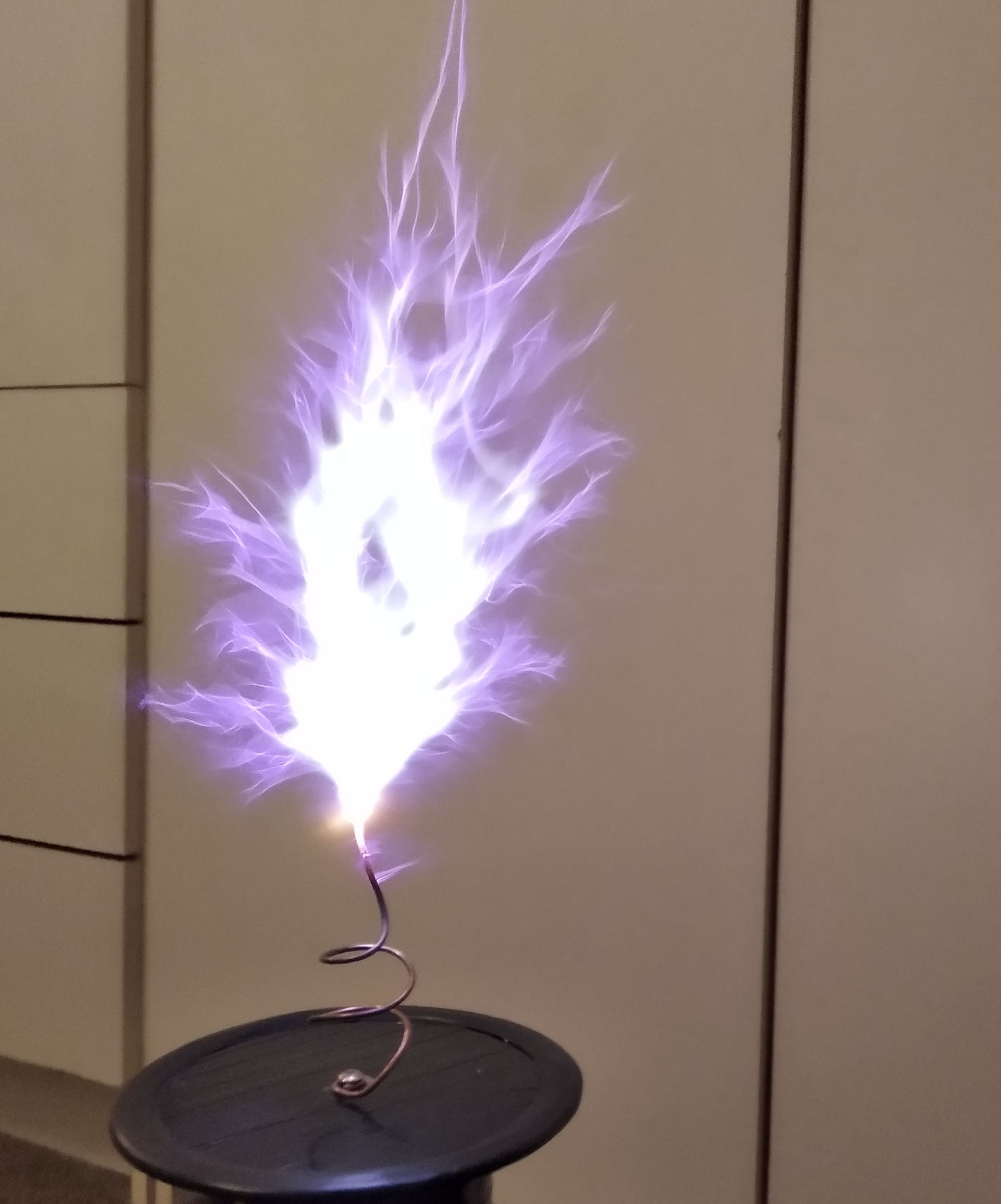
Continuous wave operation (click for full resolution)