DISCLAIMER! High voltages are present in this device, strong electromagnetic fields are emitted during operation. The device should NEVER be run without proper shielding. I refuse to take ANY responsibility for any possible injuries, legal problems, property damage or deaths, anything you find here is provided WITHOUT ANY WARRANTY, you do everything AT YOUR VERY OWN RISK!

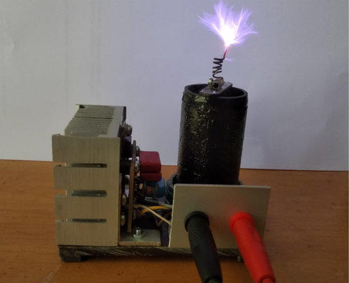
Entire device - operating (click for full resolution)

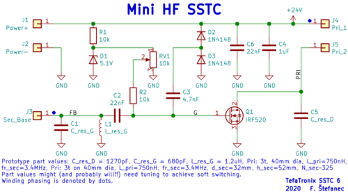
Schematic diagram (click for full resolution)
The input voltage is connected to J1, J2. Filtering/decoupling capacitors C4, C6 are connected in parallel to the input.
Parts R1, R2, D1 (Zener diode), RV1 (trimpot) form a circuit that allows setting the gate bias. The trimpot RV1 should be adjusted to the point where the circuit starts reliably, however the bias voltage shouldn't be too large to prevent destruction of the power MOSFET in case of loss of feedback.
The power stage is operating in Class C. The capacitance C5 connected parallel to the drain of the MOSFET should be chosen so that the voltage on the drain resembles a half-wave rectified sine wave. Manual tuning will likely be necessary, but an initial value can be estimated by choosing a capacitance that will resonate together with the drain capacitance ($C_{oss}$) and primary (connected to J4, J5) inductance at the secondary resonant frequency $f_{res}=1/(2\cdot\pi\cdot \sqrt{((C_{oss}+C_{res\_D}) \cdot L_{pri}) })$. The optimum capacitance will likely differ due to the MOSFET switching duty cycle, effect of magnetic coupling of the coils, non-linearities of the MOSFET capacitances, etc. The resonant capacitors should be high quality (WIMA FKP capacitors are used here) as they have to withstand several amperes of high-frequency current.
Feedback is taken from the secondary base, which is connected to J3. A resonant circuit consisting of C1, L1 and the MOSFET gate capacitance is connected in parallel to the feedback input. The voltage is clamped using parts C3, D2, D3. The capacitor C2 blocks DC voltage and thus allows the MOSFET gate to be biased through resistor R2. Due to the capacitive impedance of the voltage limiter circuit, it will likely be necessary to choose the capacitance of C1 to be a bit lower than the calculated value (680 pF works well here). Values of all parts used in the resonant circuit are written in the text in the circuit diagram. The resonant circuit corrects the phase offset that would be otherwise caused by driving a capacitive load (MOSFET gate) and increases input impedance (without L1 and C1, the feedback circuit impedance would appear to be capacitive and fairly low). C1 also decreases the effect of gate capacitance non-linearity and the effect of the Miller capacitance. It would be possible to use a better, less distorting clamp circuit in some next version. It is MANDATORY to use correct winding phasing (starts/ends of windings) - it's denoted in the schematic diagram using dots.
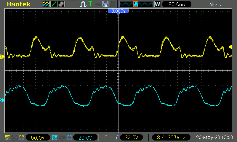
The IRF520 MOSFET is somewhat overloaded here voltage-wise (G-S peaks around 25 V, D-S peaks around 110 V with 27 V input).
PCB layout is fairly critical here. All traces should be as short as possible and the gate and drain related loops should be well separated. The circuit layout isn't published, because the board was physically modified after being etched.
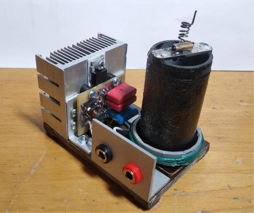
The prototype is constructed on a pertinax board. The coils are wound on polypropylene pipes. An old PC CPU heatsink is used to cool down the MOSFET (an alumina isolating pad is used), heatsink temperature during operation is around 60-70°C. The PCB was made using photo-transfer.
Values of tuning parts also depend on the input voltage (one of the reasons is that higher voltages/higher powers will lead to bigger sparks, which decrease the secondary resonant frequency). See waveforms below. This prototype is optimized for 24-27 V input voltage, this can be seen on the waveforms.
The spark/discharge is quite short, but extremely hot.

Entire device (click for full resolution)

Waveforms (yellow: drain, blue: gate), input voltage 19 V (click for full resolution)

Waveforms (yellow: drain, blue: gate), input voltage 24 V (click for full resolution)

Waveforms (yellow: drain, blue: gate), input voltage 27 V (click for full resolution)