Old ISA sound cards often do not have any decent built-in MIDI synthesis, but many of them have a 26-pin header to which an additional MIDI module can be attached. The sound of sample-based or combined syntesis is usually considerably better than FM synthesis. I was inspired to build this by the "DreamBlaster" module line by Serdaco.

Operating module (click for full resolution)

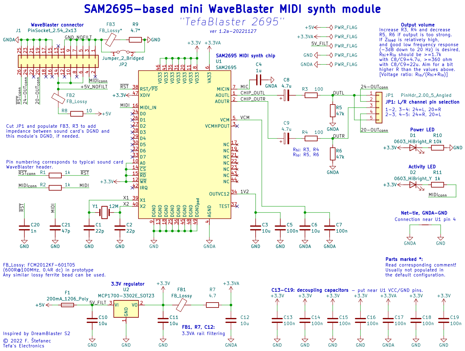
Circuit diagram (click for full resolution)
This module is based on the Dream SAM2695 chip. The SAM2695 chip is an integrated MIDI synthesis solution, containing the sample ROM, DAC, and general MIDI synthesis core. Therefore, relatively few external parts are needed. Here the chip is configured to operate in serial MIDI mode.
The power input (only the +5V rail is used) is filtered through FB2 (lossy ferrite bead), R8, C10 and regulated down to 3.3 V by the chip U2 (MCP1700-3302E regulator, others like XC6206 can probably be used too). The digital power rail is filtered using a 10 µF capacitor (C11). The analog power rail is further filtered using parts FB1, R7, C12. Decoupling capacitors are placed near the chip (C13-C19, C3-C7). The analog and digital grounds (GNDA and GND) are joined on the PCB in a single place near/under the chip. Data lines (MIDI and RESET) are connected through 1 kΩ resistors (R1, R2) and filtered with capacitors C20, C21. The RESET/PD line of the chip resets the chip on the rising edge of the signal and keeps it powered down when the signal is low. The RESET line on the WaveBlaster connector is active low. This is practically compatible. Inputs of the SAM2695 chip are 5 V-tolerant.
Output of the chip goes through capacitors C8, C9 (tantalum type for better linearity compared to ceramics) through R3, R4 to the output. To ensure zero DC bias, R5, R6 weakly pull the output to ground. To reverse the outputs, as some sound cards have the left and right channel swapped on the WaveBlaster connector, do not populate R3, R4 and populate R10, R11 (otherwise do not populate R10, R11). To decrease the output signal amplitude, put lower values of R5, R6 and increase the value of R3, R4 (or R10, R11). Increase the capacitance of C8, C9 to get good low frequency response. For an YMF719-based sound card, I found that having R5, R6, R3/R10, R4/R11 = 470 Ω and C8, C9 = 22 µF works well.
For power/use indication, LEDs are used. D1 is used for power indication and is powered through a 10 kΩ resistor, providing around 0.15 mA for a high-brightness red LED. For use indication, the data line is used, but with a 1 kΩ resistor (duty cycle will be considerably lower though). The data line is high when idle, therefore the LED (D2 - high-brightness yellow) stays off normally, and blinks when there's data going into the device.
The sound quality of the module is decent, in games that support MIDI, it's considerably better than the built-in FM synthesis, especially if the sound card has a low quality clone of the classic OPL2/OPL3 FM synthesizer. Examples of the sound of this module can be easily found online, as other modules (e.g. DreamBlaster S2, Rayer's module) based on the same chip will use the same built-in samples for synthesis. I found the ability to swap channels and change signal level on this module quite useful, if another version will be created, the appropriate resistors will be placed in a more simply available location.
The construction shown here is done using mostly 0603 parts (resistor, LEDs), except non-polarized 10 µF ceramic capacitors (0805), tantalum capacitors (case "A" - ~1206), the crystal (2-pin 5032 package), 0805 ferrite beads, 1206 fuse, and the chips, and connector. The voltage regulator is in a SOT-23 package. The main chip (SAM2695, QFN-48 0.4 mm pitch package) can be somewhat difficult to hand-solder due to the small pitch. The connector is a female pin socket, 2x13, with 2.54 mm pitch.
Version 1.2a has a jumper for channel reversal (no need to swap resistors), and the amplitude limiting resistor divider is placed on top of the PCB (easily available and labeled).
Circuit diagram, v1.2a (click for full resolution)
Module, top (click for full resolution)

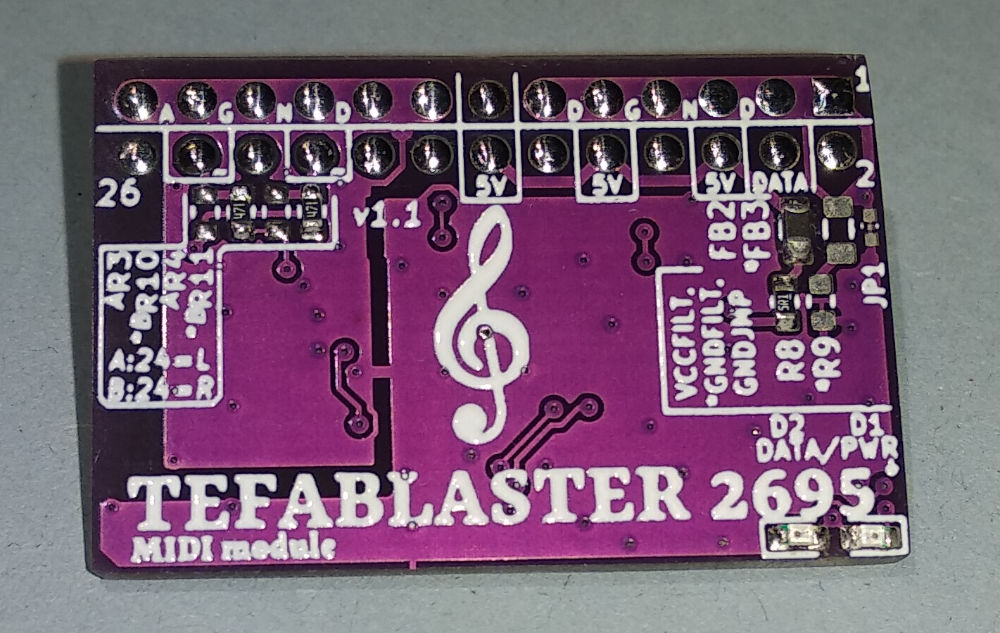
Module, bottom (click for full resolution)
Module, version 1.2, top (click for full resolution)

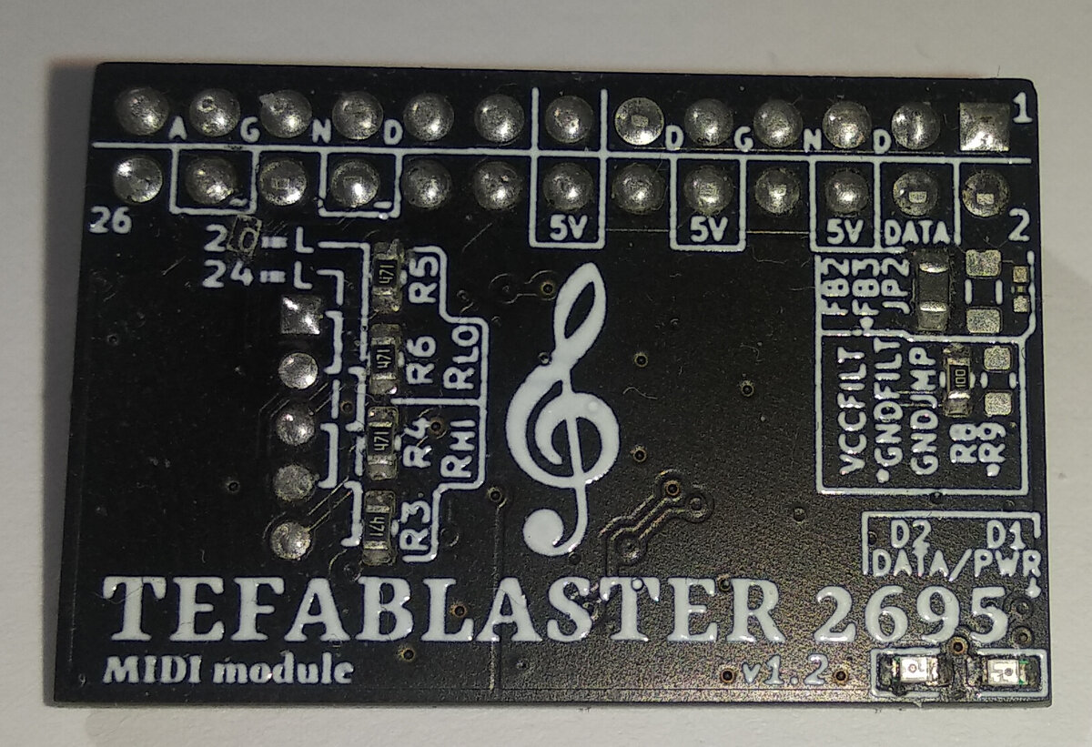
Module, version 1.2, bottom (click for full resolution)
All archives available here for download are under the Creative Commons BY-SA license, version 3.0 or newer (4.0).
Download - KiCad 6 files, .7z archive. Version 1.1 without correction.
Download - KiCad 6 files, .7z archive. Small correction in schematic, version 1.1, PCB layout unchanged.
Download - KiCad 6 files, .7z archive. Version 1.2 without correction.
Download - KiCad 6 files, .7z archive. Version 1.2a.
Download - Gerber data (verify before sending to the manufacturer!), .7z archive. Version 1.2a.
Version 1.1 without correction has one net labeled wrongly (22-OUTconn, should be 20-OUTconn). No PCB correction needed. Corrected in the updated archive above and in the schematic diagram. Version 1.2 (which will be released later in its fixed form, 1.2a) has the same error, but in silkscreen too. This is fixed in v1.2a, which is called 1.2a due to the PCB modification.