DISCLAIMER! High voltage experiments are dangerous. I refuse to take ANY responsibility for any possible injuries, legal problems, property damage or deaths, anything you find here is provided WITHOUT ANY WARRANTY and you do everything AT YOUR VERY OWN RISK!
This device was created mostly for demonstration purposes. It can drive most "normal" high voltage flyback transformers or ignition coils.

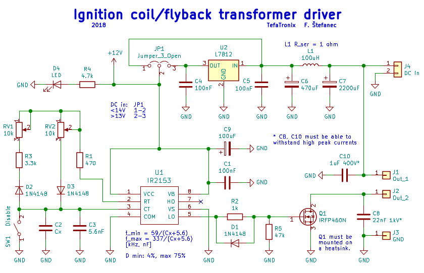
Circuit diagram (click for full resolution)
This circuit is based on the IR2153 IC. There are integrated circuits more suitable for this purpose, but I had this one already available at home. It's a self oscillating half bridge driver. I use only the low-side output. I used potentiometers with diodes instead of a single timing resistor, so I am able to adjust the off and on times independently. There's a 3.3kΩ resistor in series with the off-time potentionmeter (RV1) in order to guarantee some reasonable off time. Frequency can be changed by changing the capacitor marked Cx. I used a switch with a 1µF capacitor in order to be able to select two different frequency ranges. In this case the low frequency range is about 30-600 Hz, and the high range is 12-60 kHz. SW1 can be used to switch off the output - if the voltage on the CT pin of U1 drops below 1/6 Vcc, it turns off its output.
Capacitors C1, C4, C5, C6, C7, C9, C10 are used for filtering/decoupling. These capacitors should be close to the other corresponding parts. The inductor L1 together with C6 filter power for the more sensitive parts of the circuit. The inductor has 100 µH and 1 Ω series resistance (RLC circuits won't oscillate if R≥2*sqrt(L/C), choose Rser to be around ~1 to 2 Ω). The traces/wires between C7, C10, Q1, C8 should be as short as possible and fairly thick. Overall, it's a good idea to use short traces in this circuit where possible.
I chose the IRFP460N MOSFET because of its relatively high maximum ratings. Here it's stressed a lot by spikes from the primary coil of the connected transformer and by fairly large currents. It has to be mounted on an adequate heatsink! To limit the spikes at least a bit, C8 is connected between its drain and source (with ignition coils I use an additional 1 µF). The gate charging time is slower than the discharging time (due to R2, D1) in order to prevent C8 from discharging through the FET's channel too quickly. R5 is here to discharge the gate in case the output of U1 is disconnected.
J1 selects the input voltage. For 12 V (position 1-2, <14 V), the voltage regulator U2 isn't used. If it's set to the second position, U2 decreases the voltage to 12 volts for U1. I don't recommend going over 24 volts on the input (and 14 volts max for the IR2153 chip). A fan can be connected (recommended!) between +12V and GND. The current draw is several amperes at 12 volts with a typical flyback transformer, use a beefy power supply.
The main disadvantage of this circuit is the absence of any over-current protection. It will probably be added later.
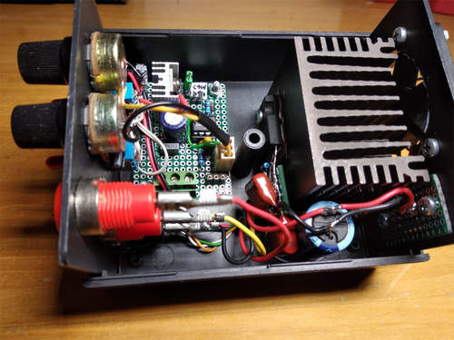
This circuit is built on an universal PCB.

Front panel (click for full resolution)

Inside (click for full resolution)

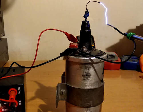
Arc - ignition coil (click for full resolution)

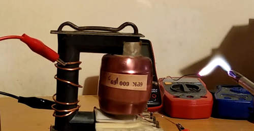
Arc - flyback (click for full resolution)