DISCLAIMER! High voltage experiments are dangerous. I refuse to take ANY responsibility for any possible injuries, legal problems, property damage or deaths, anything you find here is provided WITHOUT ANY WARRANTY and you do everything AT YOUR VERY OWN RISK!

Circuit diagram (click for full resolution)
This is a very simple circuit usable as a high voltage transformer driver (for TV flybacks, etc...). It can also be used for induction heating or wireless power transfer. It was designed by Vladimiro Mazzilli and is well known under the name "ZVS driver" in the high voltage hobbyist community. The circuit diagram above has only a few small modifications (smaller MOSFETs - IRF540 - therefore operating voltage is limited to 12-24 V), otherwise it's nearly identical to the original circuit.
Essentialy, it is an efficient, high-powered resonant Royer oscillator. The primary coil of the high voltage transformer (usually 3+3 to 6+6 turns, both parts wound in the same direction, center tapped, wound on the exposed part of the transformer's ferrite core) is connected to connectors P1, P2, P3. This coil forms a resonant circuit with the two capacitors (C1 and C3 - they must be very high quality, because high currents (10s of amperes) flow through them! The capacitors and MOSFETs must have a voltage rating of at least 4*Vin. I usually use a capacitance rating of 220 nF to 1 µF) that are connected to the coil. Because of the resonant circuit, the voltage waveform across the primary coil is (approximately) a sine wave.
The choke (inductor) L1 supplies almost constant current to the resonant circuit and blocks AC. It must be rated to withstand the input current (often ≥10 A). The MOSFETs switch when the voltage across them gets close to zero. Diodes D1, D2 with resistors R1, R2 provide gate drive. When one MOSFET is turned on, it pulls the gate of the opposite MOSFET down. Therefore, it's impossible for both MOSFETs to be on at the same moment. The Zener diodes (D3, D4) prevent gate voltage from going too high (in case of high supply voltage).
The operating principle is very simple. Waveform photos are available below. Oscillation is kicked on by differences in the components (different gate threshold voltage...) and noise. After the oscillation is sustained:
Advantages:

Assembled circuit board (the heatsinks barely get warm at over 200 W) (click for full resolution)

Waveforms - single MOSFET (upper: G-S, lower: D-S) (click for full resolution)

Arc - 12 V in, small unrectified plasma ball flyback transformer (click for full resolution)

Arc - 24 V in, plasma ball transformer (click for full resolution)
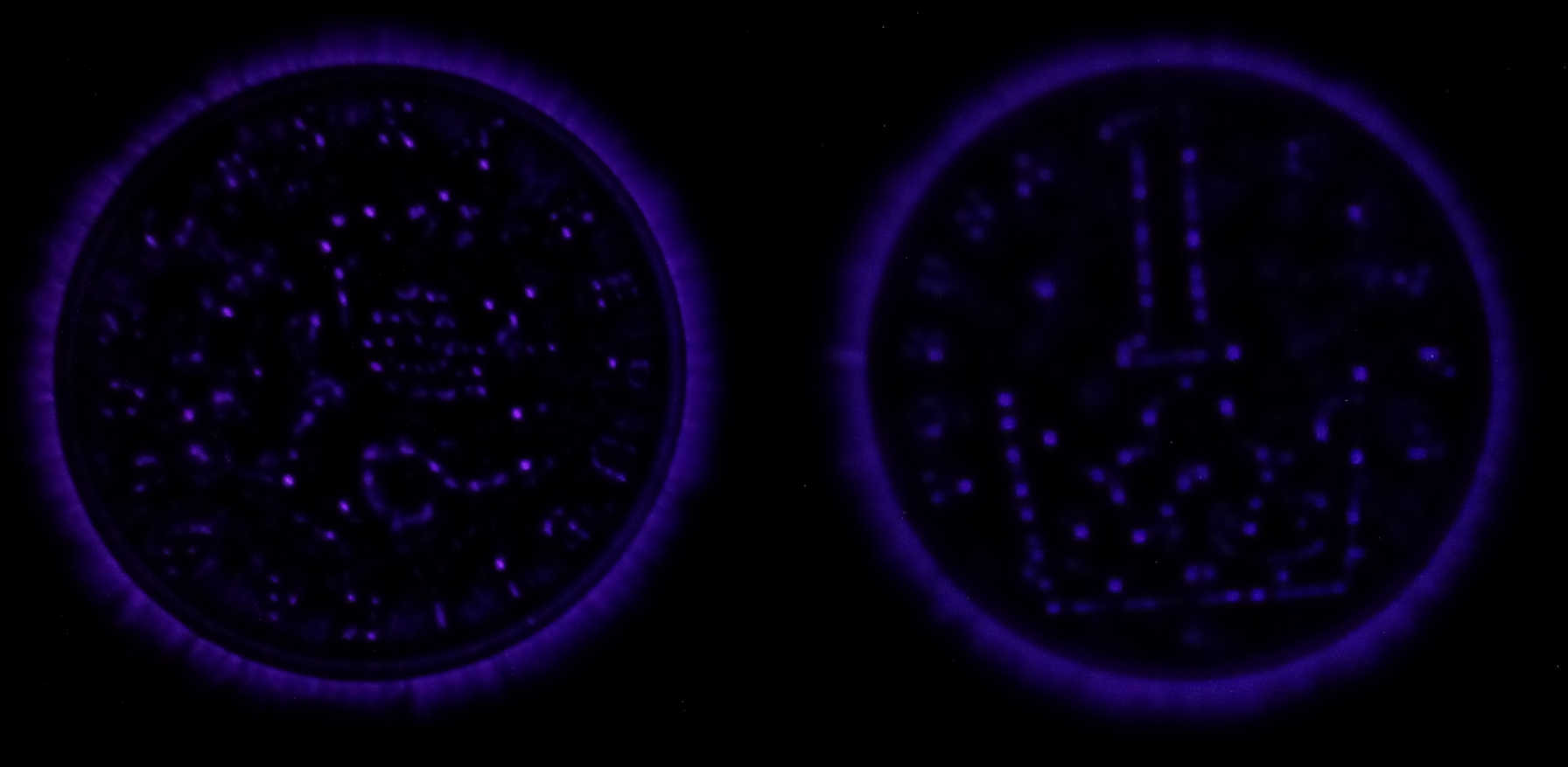
Kirlian photography of a 1 CZK coin (AC flyback) (click for full resolution)

Kirlian photography of a key (AC flyback) (click for full resolution)