This device is powered using mains voltage. You do everything at your own risk.

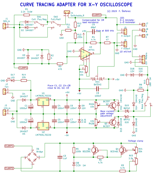
Schematic diagram (click for full resolution)
This is a tool for measurement of I-V curves (ampere-volt curve, current-voltage characteristic) using an oscilloscope with a X-Y mode. It is usable for measuring the I-V curves of diodes, transistors and other parts.
This tool is powered from a transformer with two independent secondary windings (30 V and 12 V). The transformer is powered from mains voltage through a corresponding fuse. It is recommended to use a transformer where the windings aren't wound on top of each other (minimal pri-sec capacitance is desirable). The 12 volt winding powers the measurement electronics (op-amp, etc.). Diodes D4, D5, capacitors C1, C2, C4, C5 and voltage regulators U1, U2 (7809 and 7909) form a symmetricacl power supply with ±9 V output.
The 30 V winding is used to power the measured part itself. Considering the waveform to be sinusoidal, the amplitude is 42.4 V. The current is limited with an external resistor connected to J4 (100 Ω default, extra resistors - 47, 100, 220, 470, 1000, 2200 Ω - are connectable in series using the front panel switches). This limits peak current to approx. 10 to 400 mA. There is a fairly big power loss (up to 9 W average with 100 Ω selected), the resistors must be properly rated. A small cooling fan is also used here. Switches SW1 and SW2 select full/half wave mode (and which half-wave to use, positive or negative). The device under test is connected to J7 and J9. The current is sensed using R2 (1 Ω). Diodes D3, D7 clamp the max. voltage across R2 to approximately ±0.7 V. The diodes will conduct negligible current until approx 0.4 to 0.5 V is reached (under normal temperature). The signal is then amplified using U3 (in the built version, CA3140 was used instead, because of better parameters). Capacitors C6, C7 are placed close to the op amp. D11 (dual Schottky diode) is used for protection. The op-amp is used in inverting mode (the voltage measured correspondes to the current from J7 to J9, but with the opposite sign). The gain is -10. Resistors R11, R12 and R13 (R13 is two 470 kΩ resistors in parallel) compensate the current draw of the oscilloscope connected to J5 (1 MΩ is assumed). The offset is adjusted with the trimpot RV1. J5 is the X output (voltage), J6 is the Y output (10 mV/mA).
To clamp the voltage across the DUT, the circuit consisting of D6, C3, R5, D8, Q1, Q4, R6, R9, RV4, RV3 is used. It is necessary to put Q1 on a small heatsink. The voltage is rectified using the diode bridge D6. When the voltage between the base of Q1 and anode of D8 exceeds approx. 4 V, Q1 starts conducting. The voltage is set using potentiometer RV4, which forms a voltage divider together with RV3 and R9. Q4 acts as a voltage follower (current buffer). In the build, a MJE13009 was used in the place of Q1 - it is quite overdimensioned, but I had it on hand. The maximum voltage is set using RV3.
To measure characteristics of transistors, an additional base/gate supply is present. The base or gate is connected to J8. The current is limited using R10 (in the built version a switch is added - to make it possible to select a higher resistance). The voltage/current is adjusted using RV2 (a dual tandem potentiometer is used). A milliamp meter should be connected between pins 2 and 1 of J10. For measurement of MOSFETs (voltage mode), pins 2 and 1 of J10 should be shorted and a voltmeter together with a parallel capacitor (1 to 10 µF) should be attached between them and pin 3. The extra parts are here mostly for protection purposes.
This device works quite well, but isn't perfectly accurate. The main board isn't shielded from the transformer in the photos. It is necessary to add shielding between the transformer and the board (or to at least add more compensation circuitry), else the measurements will be considerably distorted!
A single-sided circuit board is used. KiCad files are available for download here.

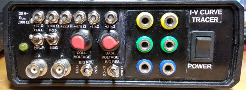
Front panel (click for full resolution)

Inside (click for full resolution)

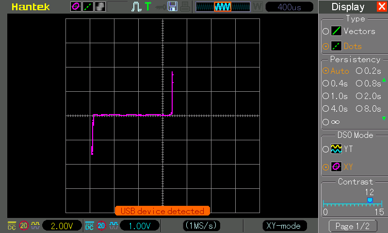
Zener diode measurement (click for full resolution)

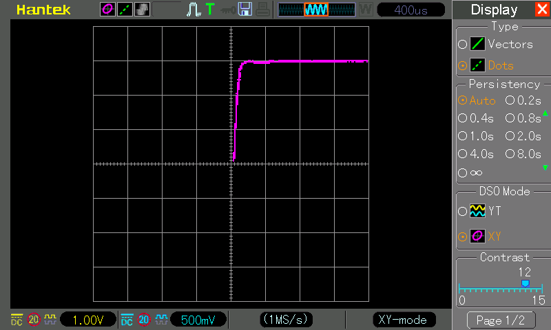
NPN measurement (click for full resolution)