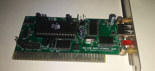
Most computers of the 486 class or older do not have any PCI slots, so if USB support is desired, classic widely available PCI USB cards can not be used, and moving larger amounts of data using floppy disks or by removing the hard disk is very unpractical. A possible solution is an USB ISA card that supports mass storage devices. Those cards are very uncommon. This card is based on the CH375B integrated circuit made by W.ch and allows a classic USB flash disk to be used. This card also has a socket for an "option ROM" chip for BIOS extension. The disadvantage is that with the basic drivers, only mass storage devices are supported.

Assembled card (click for full resolution)

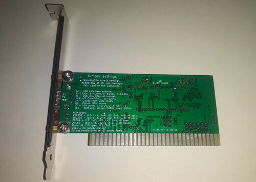
Assembled card, bottom side (click for full resolution)

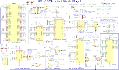
Schematic diagram (click for full resolution)
The heart of this card is the chip CH375B. The circuit diagram is based on the reference design provided by the chip manufacturer. The CH375B can communicate in UART or parallel modes, here the parallel mode is used, which is enabled by grounding TXD (when the chip detects that the pin is grounded on startup, it will switch into parallel mode). U3 (74LS245, bidirectional bus driver) electrically separates the CH375B from the ISA bus and boosts its drive capability. ISA signals A0, IOR (I/O read), IOW (I/O write), RESET go directly to U4, IOR also sets the direction of 74LS245.
Address decoding is done using chips 74LS138 and 74LS32 (respectively a few of its gates). The address is selected using the jumper block J2 (possible values 230h, 240h, 250h, 260h). Only the bottom 10 address lines are decoded, which is enough for I/O purposes as long as another card, whose low address line settings might overlap, isn't installed. Address lines A1, A2 are ignored. For example, if the address is set to 260h, the card will take addresses 260h-267h. The jumper block J3 is used to set the interrupt (off, IRQ3...IRQ7 - 1-2: off, 3-4: IRQ3, 5-6: IRQ4...), the interrupt can be disabled (with proper driver settings) with a small performance penalty. The IRQ output of the CH375 is active low, while the ISA IRQ lines are active high, so for inversion, Q1, R2, R5 are used, and buffered by U1A. Warning - Q1 (BSS138) is extremely ESD sensitive, using a protected version is recommended.
External (J6) or internal power (ISA) can be selected using the jumper J7. USB power is filtered using a lossy ferrite bead (FB1), protected using F1 (polymer resettable fuse), and filtered using C11-C13. The lossy property of the electrolytic capacitors helps dampen unwanted oscillations/noise. ESD protection is also present, U6 (USBLC6-2SC6) - it is not strictly mandatory (pins 1-6, 3-4 can be jumpered), but strongly recommended. C13 and U6 should be close to the USB connector. Capacitors C15, C16 are recommended by the CH375B datasheet, should be placed close to the chip, and seem to be necessary, without them, there are issues with data corruption.
The main chip's working frequency (12 MHz) is generated by its built-in crystal oscillator, to which a crystal is connected (Y1) together with loading capacitors C8, C9. Parts Y1, C8, C9 should be close to the chip. The CH375B has a built-in 3-volt regulator for USB, which only needs an external capacitor (C7). Blocking capacitors generally (C2, C4-C7, C10, C14) should be placed close to respective chips and some attention should be paid to reasonable design rules for digital circuits.
An optional ROM ("BIOS option ROM") can be installed as U7 (a socket is recommended) and can be either an EPROM, EEPROM or FLASH, series 2764, 2864, 28256, 29256 (variations can be found as 27C64, 28C64, 28C256, 29C256, AT28C64, AT28C256, AT29C256). The programming algorithm is different for different chips. The ROM chip type is selected with jumpers J8, J10, J12, jumper description is in the schematic. Bad configuration (especially J8) can lead to issues and in an extreme case even to board/card damage. J11 selects the base segment for the ROM (C800h if installed, otherwise D800h). The ROM address range is C8000h-CFFFFh or D8000h-DFFFFh for a 32 kB ROM, C8000-C9FFFh or D8000-D9FFFh for an 8 kB ROM. J5 enables/disables the ROM and J4 enables/disables ROM writes (only for 28xx and 29xx series). The ROM data lines aren't buffered, using a type with weak outputs isn't recommended.
Logic ICs of the 74LS... series (74LS32, 74LS138, 74LS245, 74LS688) can be exchanged to 74HCT... (74HCT32, 74HCT138, 74HCT245, 74HCT688). It is even recommended - the HCT series is fast enough and consumes less power.
The prototype was build mostly using SMD parts in 0603 packages. Logic chips are in SOIC packages. All jumpers are typical, with a 2.54 mm pitch. 10 µF non-polarized capacitors are ceramic, 1206, >16 V. The ferrite bead is in a 0805 package, type FCM2012KF-601T5, but the type isn't critical (lossy, recommended parameters: current ≥500 mA or even better ≥1 A, impedance ≥100 Ω at 100 MHz). The fuse is resettable, polymer type, 1206. All electrolytics here are typical THT parts with a 5 mm diameter.
Versions 1.0 and 1.0a only have minimal differences (slightly tuned part values). This article is talking about the original (1.0) version. For example, the pull up resistors R1, R2, R3, R5, R9 (1 kΩ) have an unnecessarily low resistance and it's better to use 2.2-4.7 kΩ.
Sadly, bracket dimensions/drawings have been lost.
It is better to use a gold plated edge connector instead of tinned (e.g. HASL), especially if the motherboard uses golden (as opposed to brass, bronze or nickel plated) contacts, to decrease degradation of the gold plated contacts. ENIG surface finish is enough for this, the gold layer is thin, but the nickel layer is thick enough for protection (approx. 5 µm), even though contact resistance will be a bit higher with the gold layer worn out.
The supported systems are MS-DOS (or other DOS) and Windows 9x (testing was done on Windows 95, but the driver should likely work with 98 or 98SE too). The driver from the chip supplier can be used and in DOS it can be loaded in CONFIG.SYS, using a similar line to this:
DEVICE=C:\DRIVERS\CH375DOS.SYS @260 #03
where @260 sets the address and #03 sets the interrupt. Speed can also be specified in the format %03, the lower the number, the faster it will be - but I don't recommend changing it. For no interrupt, specify #00.
Windows 9x has an issue, where after loading the driver in CONFIG.SYS, MS-DOS compatibility mode is forced for all disks, which decreases system performance. This can be worked around by loading the driver in AUTOEXEC using a utility like LOADSYS or DEVLOAD. The likely cause of this problem is that the system tries to load some drivers (such as IFSHLP) only after loading CONFIG.SYS, and there is some issue with the order of loading the drivers. To load the driver in AUTOEXEC.BAT, a line like this can be used:
C:\DRIVERS\DEVLOAD /H C:\DRIVERS\CH375DOS.SYS @260 #00
A new disk letter will appear in the system. If no flash disk is connected, a "device not ready" error will appear, otherwise it will work normally. I recommend disabling caching for that driver letter. Also, the classic FORMAT utility can not be used. For DOS before 7.10, FAT16 has to be used.
The card was tested in several computers, several pieces were built and one is now used in a DECpc LPv+ 425sx for almost a year with no issues. However, the article and all attached files are provided with no warranty at all.
Utility DEVLOAD (GPL v2) and driver CH375DOS.SYS.
Kicad 6 files, Gerber files, versions 1.0 and 1.0a.
- hardware design license is Creative Commons BY-SA 3.0, or newer (4.0).