Preliminary version of article - more information will likely be added.
This is an interposer inserted between a 3-volt only 5x86/486 CPU (e.g. Am486DX4, Am5x86-P75...) and a 5-volt only motherboard. These CPUs typically tolerate 5-volt logic inputs and their I/O is TTL compatible, so it is enough to regulate just the Vcc voltage.

Circuit diagram (click for full resolution)
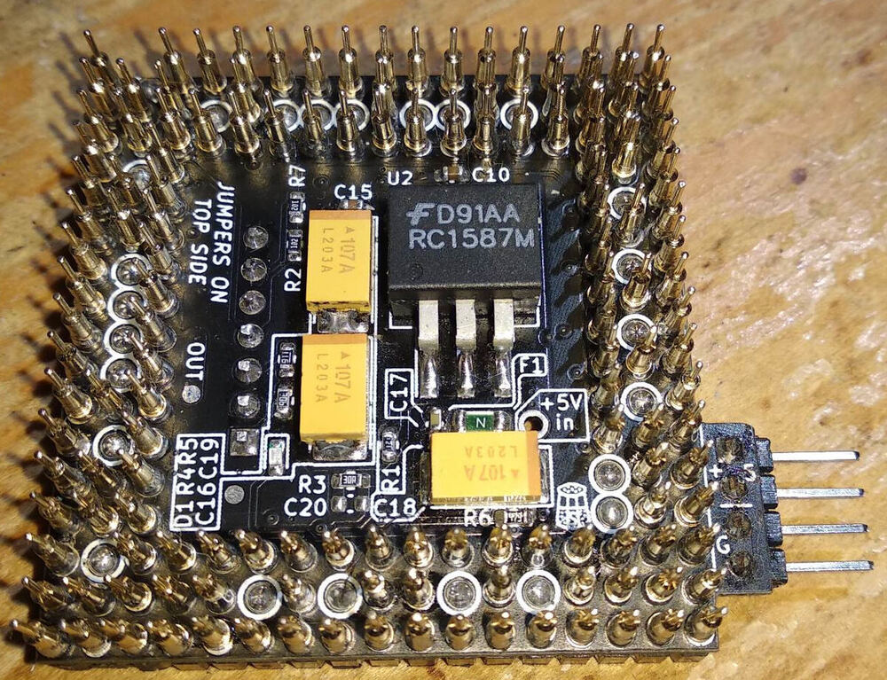
The input voltage from the +5V rail (taken for example from a HDD Molex connector) of the power supply is connected to the connector J1. The interposer will not work without this power input. For protection, a 2A fuse is used. Then, there is some filtering (tantalum capacitors C17, C18). The voltage is regulated using U2 (LT1084-ADJ or compatible - e.g. RC1587M). The output of the voltage regulator is filtered using C16, C19 and a lot of smaller ceramic (MLCC) capacitors.
Ceramic capacitors C1-C15 are placed near the CPU power pins. They act as decoupling/a local power source for short spikes. Some voltage regulators are unstable with a low ESR high capacitance capacitor on their output, so it might be necessary to lower the capacitance of C1-2, 7-8, but with a RC1587M regulator, voltage regulation is stable even with C1-2, 7-8=10 µF.
The output voltage is set using resistors R1, R3-5 and can be calculated as $V_{out}=V_{ref}\cdot({1+\dfrac{R_{lo}}{R_{hi}}})$,
where $V_{ref}$ is 1.25 V, $R_{lo}$=R3, $R_{hi}$=R1/parallel combination of R1, R4/parallel combination of R1, R5, depending on jumper settings (JP1 pins 1-3: open/1-2/2-3), giving voltage choices of 3.33/3.46/3.61 V, close to nominal CPU voltages of 3.3/3.45/3.6 V. 1% or better accuracy resistors should be used.
For cache (WB/WT) and multiplier settings, jumpers can be used - pins 4/5 and 6/7 on the jumper block J1. Possible combinations are mentioned both here and in the schematic diagram. This is based on information from AMD datasheets.
All Vcc pins except VCC5V and pins B13, R17 are disconnected from the motherboard. All other pins are connected to the motherboard using pins soldered on the bottom of the interposer board. The CPU socket was constructed using gold plated precision/"machined" 2.54 mm sockets. Individual pins removed from those sockets were used as the bottom pins.
This interposer device was tested with a classic Am486DX4, an enhanced Am486DX4 and an Am5x86 and works well with these CPUs, at least according to my (preliminary) testing.
CPU pin A1 (marked by a cut corner on the CPU) is marked here with a silkscreen triangle. Putting the CPU or interposer into the socket the wrong way can damage the CPU, interposer and/or motherboard!
Some more information (thermals...) is in the text in the schematic diagram.
The circuit board was made by JLCPCB - 4 layer, 1 mm thickness, JLC3313/2313 substrate (for this application, substrate type is not critical).

Interposer - top, CPU sockets (click for full resolution)
Interposer - bottom, to MB (click for full resolution)