This controller/driver is usable for driving addressable LED strips (with WS2812, WS2812B or similar RGB LEDs, which contain a controller chip with three PWM outputs for R, G, B + circuits for control and data transfer) and chains (based on WS2812, WS2811 or equivalent chips) with length from 5 to 60 LEDs. Several modes are available, some of them sound (music) controlled. The heart of this circuit is the ATtiny85 microcontroller.
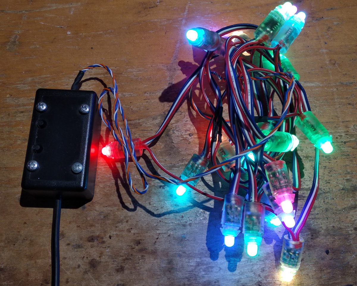
Finished device with an attached LED chain (click for full resolution)
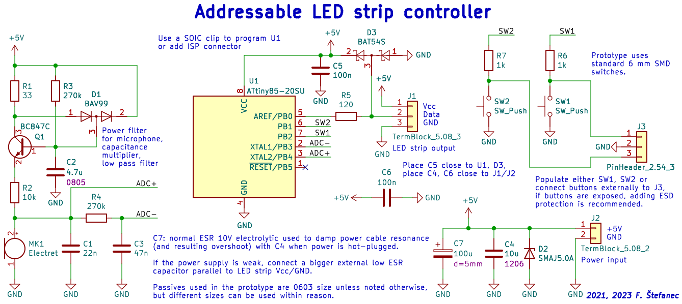
Schematic diagram (click for full resolution)
This circuit is based on the ATtiny85 microcontroller (U1). A programming connector isn't included in in the schematic diagram, the microcontroller was originally programed using a SOIC clip, later a pogo pin connector was added into the finished prototype using thin wires. To make programming easier, a classic ISP connector can be added (to pins MISO, MOSI, SCK, RST, VCC, GND according to the datasheet of ATtiny85 and the pinout of the AVR ISP connector). C5 (100 nF), a decoupling ceramic capacitor, is placed close to its VCC/GND pins.
Data for the LED strip are taken from pin 5 (PB0) of U1. A resistor is placed in series (R5, 120 Ω) for short-circuit protection and EMI radiation reduction (in case further reduction is needed, a small capacitor can be placed from the node after the resistor to ground). The double diode D3 works as ESD protection and must be placed close to C5. The LED strip is attached to the connector J1. A ceramic capacitor should be placed close to the power pins of J1. J1 is a classic 5.08 mm pitch PCB mounted terminal block.
Power (5 V) is connected to J2 (a 2-pin terminal block). Capacitors C4 (10 µF ceramic) and C7 (100 µF electrolytic) are used for power filtering. The electrolytic capacitor is added to limit voltage overshoots when connecting the device to an already turned-on power supply, as it damps the resonance of the cable inductance with the input capacitance (ceramics on board and strip) due to its higher ESR (without C7 and the transil, with an approx. 1 m long cable, the voltage overshoot was up to 60-70 %, with this variant, it's approx. 5 to 10 % - this is a well known problem with big ceramic/foil/other extra low ESR capacitors on power inputs of devices). The input is protected against overvoltage transients using the transil D2 (SMAJ5.0A). There is no onboard overcurrent protection; a fuse should be added or only a protected power supply should be used.
Buttons SW1, SW2 are used to switch modes. If these buttons are not populated onboard, buttons can be connected externally through J3. In case conductive parts of the buttons can be touched or nearly touched, ESD protection should be added (for example CESDBLC5V0AP or similar, or at least Zener diodes rated about 8.2 V parallel to the buttons, anodes to ground).
Noise reduction of microphone power is done by the circuit comprised of R1, R3, C2, D1, Q1. The transistor Q1 is used as current strenghtening (voltage follower), so reasonable values of capacitance and resistance can be used. R1 limits the charge current, the double diode D1 charges/discharges C2 if the voltage on it is further than approx. 0.6 V from the power rail. R3 and C2 work as a low-pass filter (-3 dB: 0.13 Hz). The microphone (reference MK1) is a classic electret microphone and is powered through R2 (10 kΩ). The dynamic impedance of a classic electret microphone is several kΩ, if we consider the impedance of MK1 and R2 to be mostly resistive in the required frequency range and to be about 2 kΩ, it forms a low pass filter with C1 at about 3.6 kHz for -3 dB. The filter made by C3 and R4 (47 nF, 270 kΩ, -3 dB: 12.5 Hz) is used to get the mean voltage on the microphone. The analog-digital converter in the ATtiny85 MCU is used in differential mode to sense the microphone voltage, the voltage is sensed across R4 (nodes ADC+/ADC-, pins PB3/PB4), where there will be an almost zero DC voltage due to C3. The ADC has a built-in amplifier, which is used to amplify the weak signal from the microphone.
Regarding PCB layout, it's necessary to prevent the high currents drawn by the LED strip (for 60 RGB LED and 20 mA/color up to 3.6 A peak) from creating voltage drops that get injected into the microphone signals. It is possible to take the ground for the sensitive circuitry (going to C1-3, MK1) separately and connect it in one place (which will not be connected elsewhere) close to C5/U1.
The PCB layout was done in KiCad, originally version 5, later imported into version 7, in which some notes were added and data were exported. The resulting gerber data can be used for a double-layer board, but the PCB layout is made/optimized mostly for do-it-yourself 1-layer PCBs. Passive part package size is 0603 unless noted otherwise.
The consumption of this device itself is about 10-15 mA. The microcontroller is clocked at 16 MHz using its built-in oscillator.
The program is written in C and assembly, compiled using avr-gcc, developed in Code::Blocks IDE. Both the HEX output for programming and source code are available for download lower.
Button 1 is used to change modes, button 2 is used for brightness adjustment. There are 8 brightness levels and 12 modes (effects). Pressing and releasing a button will do the corresponding change of mode or brightness. If the last option is selected, another press will select the first option again. The built-in EEPROM is used as non-volatile memory to hold settings while the device is powered off.
Pressing both buttons for ≥2 s saves the current choice of mode and brightness into the EEPROM. The saved mode and brightness will be restored the next time the device is powered on.
Effect list, first three are music controlled:
Random numbers for effects 11, 12 use a modified Xorshift algorithm to which some truly random data (LSb of some ADC samples) are inserted.
Settings mode can be entered by holding both buttons before powering the device on:
To limit drawn current, if the LEDs display white, the maximum PWM value is decreased. Even with 60x WS2812B LEDs, the current should be less than approx. 2-2.5 A.
Fusebit settings: HFUSE: 0xdd, LFUSE: 0xf1, EFUSE: 0xff.
AVRDUDE command for use with the USBASP programmer:
avrdude -c usbasp -p t85 -B10 -U hfuse:w:0xdd:m -U lfuse:w:0xf1:m -U efuse:w:0xff:m -U flash:w:'/path/to.hex'
The printed circuit board (40x30 mm) is made using photo-transfer and is mounted into a ZY-40 plastic box with M3 screws/nuts and stand-offs. The box is covered with copper tape under the circuit board for better electromagnetic interference immunity. A copper spring is attached to the PCB, touching the copper tape. This is somewhat excessive, the EMI protection isn't so critical. The PCB was made quite quickly in a home lab, which is, sadly, very visible. The contact pads for pogo pin programming on the top side of the PCB is attached using thin enameled wires.
The prototype is powered using USB. This isn't ideal due to the somewhat higher input capacitance (exceeding the USB specification of 10 µF) and high current draw with higher LED counts. USB type A officially outputs 0.5 A (USB 2) or 0.9 A (USB 3) after negotiation (in practice, drawing the current without negotiation isn't usually a problem), or more with DCP and other charging standards. Most common USB ports can supply an ampere without issue and the USB specification mandates overcurrent protection for the source. In practice, these non-idealities weren't a problem (the device was tested on several USB chargers, on a Latitude 5490 laptop, on several desktop computers with no issue), but still, you do this on your own responsibility. For USB operation, I recommend using less LEDs (≤30) or only a strong enough, good quality adapter. A thick power cable from a faulty laptop charger was used here, with a quality USB connector soldered to its end.
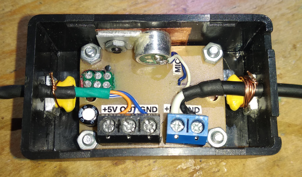
Inside (click for full resolution)
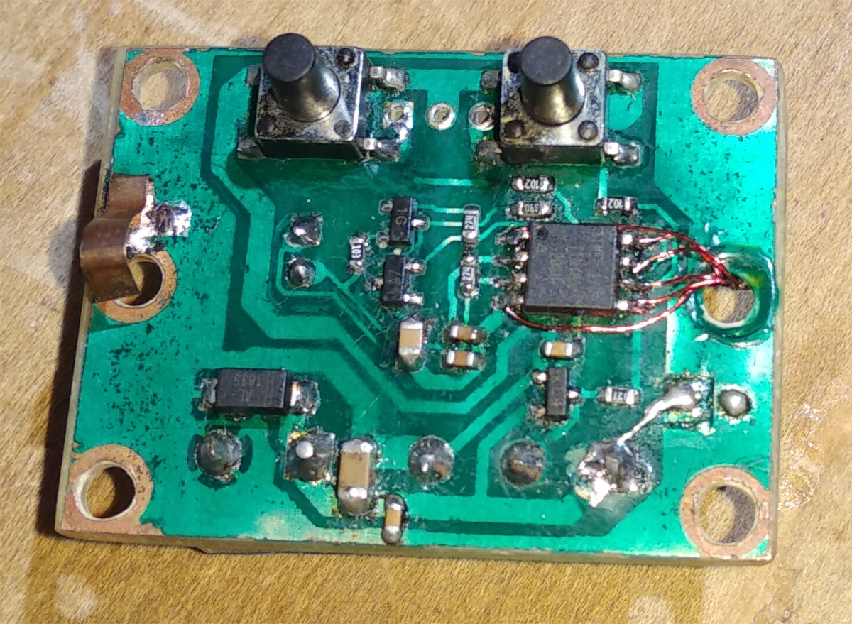
Circuit board (click for full resolution)
ZIP archive - KiCad 7, gerber data, program (HEX and source code). The source code is licensed under the BSD license, KiCad/Gerber data under Creative Commons 3.0 Attribution.